
|
k1.spdns.de / Develop / Hardware / K1-Computer / K1-Bus / |
| Blurb | Basic system | Bus lines | Bus cycles | Wait | Reset | I²C Bus | Dimensions | Example I/O board | Example CPU board | Archive |
|
|
k1.spdns.de / Develop / Hardware / K1-Computer / K1-Bus / |
| Blurb | Basic system | Bus lines | Bus cycles | Wait | Reset | I²C Bus | Dimensions | Example I/O board | Example CPU board | Archive |
Version 1.00
Last edited: 2014-10-21
 The K1 bus ia a Peripherals bus for homebuilt computers with any CPU, it may even be homebuilt too. It is not intended to access random access memory. RAM must be provided on the CPU board itself.
The bus is designed as a 16 bit bus, but may also be used as a 8 bit bus if desired.
Up to 16 peripheral boards can be addressed; or up to 8 boards if restricted to an 8 bit bus. Board selection (addressing) is done by one data line for each board, which should be selectable by jumpers.
The mechanical design is a 40 pin flat ribbon, as it was common for old IDE hard drives and for which plugs and sockets are cheap to buy. Signal wires are not interleaved with ground wires, therefore the bus should be kept short. The best is to fit sockets in exactly the distance which the boards will be fitted later.
Electrically the bus is designed for CMOS chips. Either those with CMOS level or those with TTL level, though mixed operation will probably shift some timings. Important is to keep the total load of all connected boards low enough that the bus lines can be driven with standard CMOS chips directly.
Each board can provide driver code in a I²C EEprom. Such boards can be used in any K1 bus system without configuration or driver installation. The CPU searches and installs the drivers from all connected peripheral cards at boot time. The drivers are written in a bytecode which can be translated into machine code at boot time or which can be interpreted by a forth-style interpreter at runtime. Boards which are designed for one system only do not need to provide a driver eeprom if the driver code is stored in the system rom.
The maximum data rate is roughly 32 MB/s achieved by 16 mio. 16 bit transfers per second. Whether this speed is achieved depends mostly on the CPU. A Z80 CPU with 4 MHz clock speed may reach 250 kB/s.
There is only one bus master: the CPU board. If someone wishes a DMA controller this must go on the CPU board. An external DMA controller would have made the design much more complicated.
Before data can be transmitted, the card must be /selected. This is done by a special i/o cycle with the card's dedicated data line pulled low. Thereafter all data transfer on the bus goes to and from this card until another card is selected.
Each board has it's own priorizable and maskable interrupt. An interrupt is initially signaled on the collector line /irpt. Next the CPU asks with an /rd_irpt cycle for the actual interrupt source and disables with an /wr_irpt cycle all interrupts of this and lower priority until interrupt handling finishs.
6 address lines A0 to A5 are used to select registers on the peripheral cards. 8 bit systems only need to implement 4 address lines. 8 bit CPU systems can be extended to 16 bit systems basically by adding two 8-bit latches.
The absolute minimum system consists of only one CPU board with CPU, boot rom and ram. A microcontroller is also possible. This card should be "stand-alone" executable at least for testing purposes. Additionally it may contain a timer/counter for the system time base, debugger support, such as reset and debug button and possibly a serial port to a terminal or PC, though everything of this could also be provided on an extension board.
• CPU, RAM and ROM, or all-in-one in a microcontroller
• Pull-up resistors for: /wait, /reset, /irpt and i2c_data
• Power-on reset
• Connection for power supply
Optional:
• System timer/counter
• RS232 terminal
• Watchdog timer (interrupt, NMI, or reset)
• Reset button and connection for external switch
• Debug button and connector for external switch (interrupt or NMI)
• Heart-beat LED and connector for external LED
• Supply of +5V
Optional:
• Power-off interrupt
• Power LED and connector for external LED
• On/off switch and connection for external switch
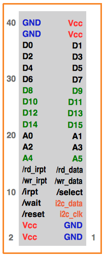
D0 … D15    Data to and from the peripheral card
A0 … A5     Register address on the peripheral card
/select     Select board
/rd_irpt    Request interrupt status
/wr_irpt    Write interrupt enable masks
/rd_data    Read data from the card
/wr_data    Write data to the card
/wait       Extension of bus cycles
/irpt       Interrupt
/reset      Restart
i2c_clk     I²C clock line
i2c_data    I²C data line (bidirectional)
GND         4x Common ground for signals and power
+5V Vcc     4x +5 volt power supply
There are 5 different bus cycles that are indicated by the CPU with 5 individual control lines:
/select (select board), /rd_irpt (read interrupt status), /wr_irpt (write interrupt mask), /rd_data (read data) and /wr_data (write data).
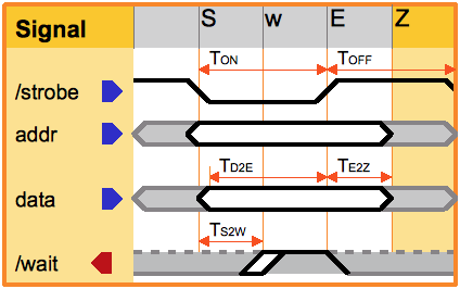
There are three bus write cycles: /select (select board), /wr_irpt (write interrupt mask) and /wr_data (write data). The bus write cycle, as the bus read cycle, consists of four time slices:
• T(Z2S): Lead time
• T(S2W): "Strobe-to-wait": Time window for a /wait signal by the peripheral card.
• T(D2E): "Data-to-end": lead time for the read data. It comprises two time slices, and is measured from the falling strobe edge. The first time slice overlaps with T(S2W) "Strobe-to-wait".
• T(E2Z): "End-to-Off": follow-up time for the register address and write data.
The strobe signal must be at least:
• T(ON): 2 time slices long active
• T(OFF): and 2 time slices long inactive.
In reality, the time slices are not the same length. The shortest time slice in a real CPU bus cycle determines its "reference clock", and the longest time slice of a peripheral card determines the CPU reference clock, up to which the board should work without testing.
On each card one data line, which should be selectable by jumpers, is set as it's "address". This is used in the /select, /wr_irpt and /rd_irpt cycle to select the board.
Data exchange with a peripheral card is always in 2 steps:
• Select the board
• Transfer data to and from the board
The /select cycle is used to select a board for subsequent data transfers with /rd_data, /wr_data and on the I²C bus.
For that the CPU performs a bus write cycle with /select used as control line.
In the mask word on the bus all bits are set, only the bit for the desired board is cleared. The mask may also be $FFFF to disable all the cards. In 8-bit systems, only the lower 8 data lines are used, hence only 8 cards are addressable.
The /select signal must be activated at least two time slices long. The mask word must be valid two time slices before and one time slice after the rising data-edge of the strobe signal.
The register address A0 - A5 is ignored. The behavior of /wait is not defined. It may be activated but the CPU may ignore it.
The peripheral cards should read their select bit with a positive edge-triggered latch, such as a 74HC74.
The CPU can turn interrupts on and off individually on all cards with a mask word.
For that the CPU puts a 16-bit mask word on the bus and performs a bus write cycle with /wr_irpt as control signal.
Set bits in the mask word block the interrupts of the respective cards, reset bits allow the respective interrupts. The mask word can also be $FFFF to disable all interrupts, or $0000, to allow all interrupts. In 8-bit systems, only the lower 8 data lines are used, hence only 8 cards are addressable.
The /wr_irpt signal must be activated at least two time slices long. The mask word must be valid two time slices before and one time slice after the rising data-edge of the strobe signal.
The register address A0 - A5 is ignored. The behavior of /wait is not defined. It may be activated but the CPU may ignore it.
The peripheral cards should read their select bit with a positive edge-triggered latch, such as a 74HC74.
The CPU can send 16-bit data to the currently selected board. For that the CPU performs a bus write cycle with /wr_data as control signal.
The address lines with the register address must be valid on the falling edge of /wr_data, then comes the response time T(S2W) for /wait. After 2 time slices T(D2E) is the data transfer edge of the strobe signal, with which the data should be transferred from the card. Thereafter, data and register address must remain valid for another time slice T(E2Z).
If /wait was activated within the response time T(S2W), the bus cycle must be frozen until the peripheral card releases /wait. Only the selected peripheral card may enable /wait. If /wait is activated outside a bus cycle, the behavior is undefined: It may be observed by the CPU or ignored.
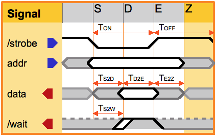
There are two bus read cycles: /rd_irpt (read interrupt status) and /rd_data (read data). The bus read cycle, as the bus write cycle, consists of four time slices:
• T(Z2S): Lead time
• T(S2W): "Strobe-to-wait": Time window for a /wait signal by the peripheral card.
Identical to T(S2D), "Strobe-to-Data": time window up to the provision of the read data.
• T(D2E): "Data-to-End": lead time for the read data.
• T(E2Z): "End-to-Off": follow-up time for the register address and switch off time for read data drivers.
The strobe signal must be at least:
• T(ON): 2 time slices long active
• T(OFF): and 2 time slices long inactive.
In reality, the time slices are not the same length. The shortest time slice in a real CPU bus cycle determines its "reference clock", and the longest time slice of a peripheral card determines the CPU reference clock, up to which the board should work.
Times are as seen on the bus:
To account for the increased capacitive load on the bus, you should start with the normal gate delays for all bus output drivers and add about 20ns additional runtime, both on the CPU board, and on the peripheral card. (to be determined)
The CPU can read the interrupt status of all cards. For this the CPU makes a bus read access with /rd_irpt as control signal.
Here, all cards must put their interrupt status on their 'select' data line. Pending interrupts are indicated '0' active. The output should be of 3-State type, the board must drive both a '1' (no interrupt) and a '0' (interrupt).
The CPU activates /rd_irpt for at least 2 time slots and reads at the end of the /rd_irpt signal the data word with the status of all cards. The data bits must be valid for at least one time slice after the falling edge of the strobe, and no later than one time slice after the data transfer edge the drivers of the card must be high impedance again.
The register address A0 - A5 is ignored. The behavior of /wait is not defined. It may be activated but the CPU may ignore it.
Of course unconnected bits float and must be masked in the interrupt handler of the CPU.
The CPU can receive 16-bit data from the selected peripheral card. For this the CPU makes a bus read access with /rd_data as control signal.
The address lines with the register address must be valid on the falling edge of /rd_data. Thereafter comes the reaction time T(S2W) for /wait. After that, either /wait was activated, or the read data are present on the bus. After another time slice T(D2E) is the data transfer edge of the strobe signal to which the data is transferred from the CPU. After that, the register address may remain valid one more time slice T(E2Z). Latest at the end of this time slice, the drivers on the card must be high impedance again.
If /wait was activated within the response time T(S2W), the bus cycle must be frozen until the peripheral card releases /wait. Only the selected peripheral card may enable /wait. If /wait is activated outside a bus cycle, the behavior is undefined: It may be observed by the CPU or ignored.
/wait is used to slow down data transfer speed by the peripheral cards, so that even slow cards can be operated with fast CPUs.
Only the selected peripheral card may enable /wait. If /wait is activated outside a bus cycle, the behavior is undefined, meaning the CPU can observe or ignore it.
/wait can be driven with an open-gain output. For this purpose the /wait line is biased on the CPU board with a pull-up resistor of approximately 5k to '1'. Thereby, it is also possible that a peripheral card implements no wait logic and leaves /wait unconnected.
/wait should be controlled by a 3-state output, which may only be activated on the selected card. The advantage over an open-drain output is that an active termination of the /wait signal by a driver who can pull the signal to '1' level is quicker than the discharge of the wire capacitance over a – comparably high – pull-up resistor.
• /wait is not used:
The card must be able to read data after T(D2E) (2 time slots) or provide write data after T(S2D) (1 time slot). The CPU must therefore be correspondingly slow or the peripheral card be correspondingly fast.
• Operating within the meaning of '/wait':
/wait is enabled by /rd_data or /wr_data. This card works with all CPUs for which it meets the wait reaction time T(S2W) (one time slice).
• Mixed operation:
Since the register address must be valid at the same time as the strobe /rd_data or /wr_data, the card's control logic can activate /wait only for certain registers, for example, if a status register is readable immediately, but not a data register.
The reset line is a collector line that may be activated by all cards. It is 0-active and must be driven with open-drain outputs. On the CPU board, it comes with a pull-up resistor of about 5k biased to '1'.
The K1 bus includes an I²C bus. This is primarily used in the boot phase to read driver software from EEPROMs on the peripheral cards. It can also be used for other purposes, but with caution: The I²C bus is slow and during communication with an I²C device probably all interrupts must be disabled!
I²C devices must be connected in a way that they are only selectable when the card is selected.
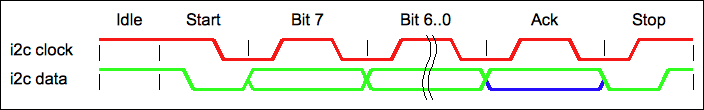
The I²C-bus consists of a clock line and a bidirectional data line. There is a master, the CPU board, which generates the clock and initiates all transfers. All other devices on the I²C bus are slaves. The master starts a bus transfer by selecting the device, then followed by a transfer of any number of data bytes. Each byte is transmitted with 8 bit MSB first. Next is a ninth Bit, in which the data receiver puts a confirmation (acknowledge) on the data line, by pulling it to '0'. Under certain conditions the device responds intentionally with not-acknowledged.
The bus is idle, when clock and data are both 1. The master sends at the beginning of a transmission a start condition, which is that it pulls the data line to 0, while the clock line is 1. Then comes one bit per clock, where the data line must only be changed while the clock line is 0. While the clock line is 1, the data line must remain stable. For the acknowledgment, the transmitter biases the data line to 1, and the receiver pulls it to 0, which is possible because the data line works with open drain outputs and a pull-up resistor. Then comes the second byte and so on until the master terminates the data transfer by generating a stop condition, which is that the data line toggles from 0 to 1, while the clock line is 1.
If the master is the receiver of the last byte, it produces in the 9th clock a not-acknowledge and then sends the stop condition. After that, the slave/transmitter switch to a power saving mode; after an Ack usually more bytes are transfered.
If data was sent to the EEprom, it is busy for a while with the programming of its EEprom cells. During this time it is unresponsive and does not generate an acknowledge on the data line. From this behavior you can tell when it is accessible again.
The I²C protocol is specified for 100kHz and 400kHz, but on the K1 bus only 400kHz-capable devices should be connected. The suggested pull-up resistor for the data line at 400kHz is 2kΩ.
At boot time, the CPU reads the card drivers from the I²C EEprom of all cards. For this the CPU selects the card with a /select bus cycle and then tries to read the EEprom at the address %1010.0001. This is the address for 24C02..16 EEproms, 24C65 EEproms or 24C128/256 EEproms if their address pins E0, E1 and E2 are connected to '0', with declaration of a read cycle in bit 0 = '1'. Address pin E2 of the EEprom should be connected to the output of the /select latches (the 74HC74), so that from all EEproms on the I²C bus only that of the currently selected card is actually selected. All others have at their address pin E2 a '1' and would feel selected only by the address %1010.1001. Some of the 'thick' EEproms do not have the Ex inputs internally connected, here you have to interrupt the i2c_clock signal to the EEprom when the card is not selected.
The EEprom contains general data about the card, such as its name and a broad classification. Then blocks of pre-compiled bytecode follow that is either translated into machine code at boot time or interpreted at runtime.
The layout of the EEprom and the Bytecode are described in i2c-eeprom.pdf.
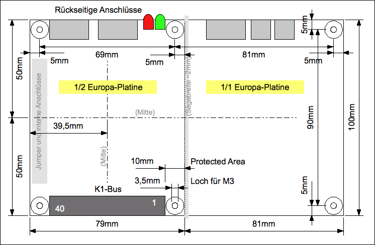
The drawing above is a proposal for the dimension of full and half-size Eurocard boards. The half-sized board is only 79mm wide to account for 2mm milling width for splitting a full-sized board.
The boards are preferably installed horizontally. Then you can mix full and half-sized board. In the corners are through holes for M3 screws or spacers. The hole diameter is also sufficient for inch coarse thread screws. Around the holes is an area 10mm in diameter in which no components and conductors are allowed. The holes must remain electrically floating and may as well not be connected to ground to prevent ground loops. However, they may be connected to the shielding of external terminals. The boards are to be bolted to M3 spacers or through M3 screws and spacers.
The preferred area for jumpers and internal connectors is left on the board.
The K1 bus connector is located centered on the 79mm wide half board and sits flush on the board edge. The rear connections are also flush with the board.
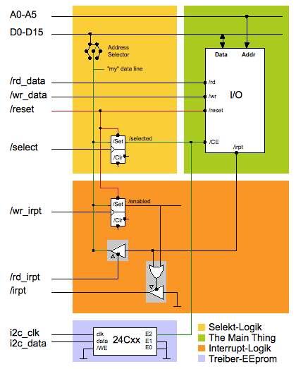 The diagram shows the basic structure of a control circuit on a peripheral card.
The large IC called I/O is what it is. If one looks at the connections here, you can see that you can connect many ICs directly 1:1.
With the address selector one of the offered data lines is set. It is genaerally ok to offer roughly 4 randomly choosen lines for jumpers. This data line is passed to the two data inputs of the 7474 flip-flops and is connected to the output for /rd_irpt.
The upper flip-flop (1/2 74HC74) stores the state of the data line when a /select cycle is performed. Its output reflects the /select status of the card.
The other flip-flop (1/2 74HC74) stores the state of the data line when a /wr_irpt cycle is executed. Its output reflects the interrupt enable status for the card.
/rd_irpt simply turns a 3-state drivers through to 'our' data line. You can use a 74HC125, which contains 4 individually controllable 3-state drivers.
Since /irpt is a collection line and may be used only with open-drain drivers pulling to '0', this circuit uses a little trick so that it can use another driver from the 74HC125 for this. The OR gate can optionally be improvised from a resistor and a diode when it is not yet available somewhere.
At the bottom of the drawing the driver EEprom is shown which is simply connected directly to the I²C bus. The address input E2, which effectively serves as a chip enable, as the /CE of the I/O IC, is provided by the /select status of the card.
An example for a CPU board with an MC68008 and SRAM can be found in ../K1-Bus 68008 CPU board with SRAM/.
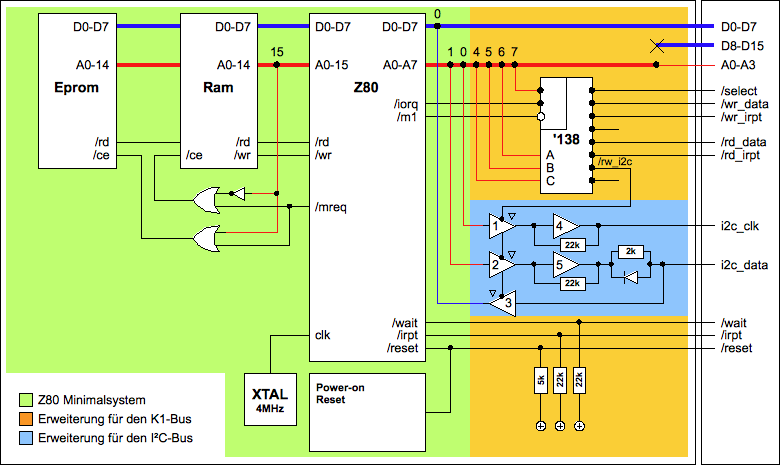
Above circuit shows a minimum Z80 system to which the control logic for the K1 bus has been added.
The minimum system consists only of CPU, RAM, EPROM, clock, reset logics and the decoding of A15 for addressing RAM and EPROM, without a timer interrupt or a PIO or SIO.
The connection for the K1 bus consists at the absolute minimum of only one IC, the 3-to-8 decoder 74HC138, and three pull-up resistors for the bus lines /wait, /irpt and /reset. The data and address lines are not buffered. This CPU card supports only an 8-bit bus, and four register address lines. D8 to D15, A4 and A5 of the K1 bus are simply left unconnected.
For switching through the 74HC138 /IORQ, /m1 and A7 are decoded. /m1 must not be enabled in order to distinguish the normal I/O access from an interrupt acknowledge cycle, and A7 is decoded so that we can still connect other I/O chips on the CPU board can.
The eight possible output lines are selected by the three address bits A4 through A6. Actually /rd instead of A4 would be quite useful, but since /IORQ and /RD are enabled by the Z80 CPU at the same time, there is a risk of glitches on the outputs when /IORQ enables the outputs of the 74HC138 before the desired output is correctly selected. With the use of 3 address bits cannot happen, because the addresses are valid before /IORQ. However, now a faulty OUT instruction coulsd lead to a bus collission.
 As shown above the I²C bus can be built with a few passive components and a 74HC367 IC. The 74HC367 contains six 3-state drivers that are activated in groups of 2 and 4 drivers. In this design the CPU uses only input instructions to control the I²C bus, even if it wants to send a bit. A1 provides the transmit bit, A0 controls the clock line. Input from the I²C data line is in D0. The sketch on the right shows the circuit that is improvised here.
Drivers 1 and 4 and drivers 2 and 5 of the 74HC367 each construct a transparent latch, the diode and the resistor in parallel convert the output of driver 5 into an open-drain output with pull-up resistor.
The circuit with the 74HC367 is not really nice, but the only one I could think of to get by with only one IC. If the CPU board has a PIO or SIO anyway, you should try to use 2 universal port bits for it. Then the I²C bus does not cost a single IC extra.
The following extension of the Z80 allows the use of 16-bit peripherals. Two 74HC574 8 bit data latches cache the data for the upper bus half. One latch is connected in direction CPU ➔ bus and one is connected bus ➔ CPU. Instead of the 74574 one can also use a 74374 or many other 8 bit data latches.
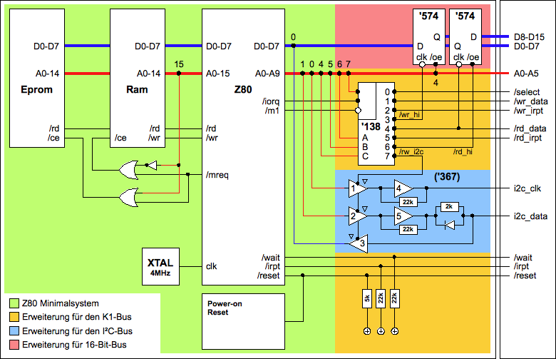
For writing a 16-bit value, first the upper byte is written to the output latch. For this one of the unused decoded lines of 74HC138 is used. This latch puts its contents onto the bus when A4 = 0. Otherwise it can not be achieved, that the data in the following 8-bit write cycle will be issued with the necessary pre-and post time.
Note: A4 is used for input 'C' of the 3-to-8 decoder, and all write control lines are connected to output 0 to 3, so that they occur at C = 0.
When reading from the bus with /rd_data the upper byte of data is always read into the read latch. Once the CPU has read the lower byte normally, the upper byte is located in the latch. This can then be read, for which the second unused line of the 74HC138 is used.
It is waived in this circuit to read the upper byte in a /rd_irpt cycle. This means that, while 16-bit peripheral boards can be connected to this CPU board, the number of expansion cards is still limited to 8. To be able to respond to 16 cards, you would have to combine /rd_irpt and /rd_data with an AND gate. ( /clk = /rd_data OR /rd_irpt <=> clk = rd_data AND rd_irpt )
| Name | Letzte Änderung | Länge | |||
|---|---|---|---|---|---|
| 2416.pdf | 2008-03-25 18:58 | 132399 | |||
| 24256.pdf | 2008-03-25 18:58 | 110699 | |||
| 2465.pdf | 2008-11-03 21:38 | 213511 | |||
| Board_Dimensions.odg | 2009-01-23 13:51 | 15055 | |||
| bus_lines.odg | 2008-12-17 15:07 | 15725 | |||
| Example_CPU.odg | 2009-01-23 14:09 | 18142 | |||
| Example_CPU_16Bit.odg | 2009-01-23 14:09 | 19042 | |||
| Example_IO.odg | 2009-01-23 14:09 | 17233 | |||
| i2c-eeprom.html | 2019-12-18 12:31 | 141021 | |||
| i2c-eeprom.pdf | 2014-04-11 22:09 | 282250 | |||
| i2c-eeprom.rtf | 2014-04-11 22:02 | 115222 | |||
|
i2c_bus_drawing_1.jpg size: 271 × 220 |
2008-12-21 11:12 | 12980 | ||
 |
i2c_bus_drawing_2.jpg size: 517 × 392 |
2008-12-21 11:11 | 43915 | ||
| i2c_bus_timing.odg | 2009-01-23 14:10 | 11968 | |||
| K1-Bus.lbr | 2014-08-21 17:26 | 428656 | |||
| Reset.odg | 2009-01-23 14:10 | 13538 |
powered by vipsi - your friendly VIP Script Interpreter
![]()
![]()