
|
k1.spdns.de / Develop / Hardware / K1-Computer / K1-CPU / IO / |
 Overview
| Control Unit
| Microcode Header
| Arithmetic Unit
| Data Registers
| Address Registers
| Expansion Bus Overview
| Control Unit
| Microcode Header
| Arithmetic Unit
| Data Registers
| Address Registers
| Expansion Bus
|
|
|
k1.spdns.de / Develop / Hardware / K1-Computer / K1-CPU / IO / |
| Overview
| Control Unit
| Microcode Header
| Arithmetic Unit
| Data Registers
| Address Registers
| Expansion Bus
|
Last updated: 2014-08-16
Questions & comments to Kio
The I/O board consists of the following units:
K1 Expansion Bus Interface | 16-to-4 Priority Encoder
Random Number Generator + Reset Circuit | Sensor Ring
DBus-to-ABus Register
The K1 Expansion Bus is used to attach extensions and peripherial boards.
The I/O bus will hopefully allow one-clock-cycle 16-bit word transfer bursts with up to 16 MHz. Since the design actually enforces an I/O transfer in one clock cycle (wait states can be added) the CPU probably must be clocked down for most expansion cards, which is implemented in the control unit.
The K1-Bus is described here. It features 16 bit i/o, 16 priorizable interrupts and an I2C bus for driver EEPROMs and the like. All on a simple 40-wire flat ribbon cable. It is designed for simplicity and hobbyists-grade high-speed. I am also thinking about using a RAM extension card for memory expansion. :-)
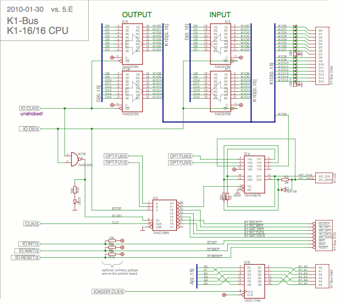
The four 74AC573 transparent registers are used as drivers because i don't have bus drivers in 74AC. As with the address bus to data bus bridge i do not use bus transceivers because of the timing requirements for the 3-state outputs to the data bus.
The K1 bus data lines are pulled low with resistor networks to allow reading of 8-bit wide data without the need to mask off the upper 8 bits manually.
The load clock IO.CLK and the output enable line !IO.OE, are combined to form one enable signal for the 74AC138 3-to-8 decoder which provides the 6 strobe signals for the K1 bus. Another enable input is attached to the CPU main clock CLK to strobe the signal to the second half of the instruction cycle. !IO.OE and two option select lines are used to select the desired strobe signal. The clock signal IO.CLK is not strobed with the CPU's main clock CLK on the control unit, as opposed to most other load clocks, so it has the same timing as the output enable signal, which stretches along the whole main clock cycle. (with 2 gate delays, if i recall it correctly.) This is required for the strobe generation and driver enables of the I/O unit.
For I/O input cycles it is sufficient to execute one instruction cycle. For I/O output the data hold time after the strobe must be created manually by appending a dummy I/O out cycle to the unused strobe pin in order to keep the output drivers driving the output data for one more clock cycle. Else the data hold time will only be approx. 10 ns. This may be enough for specifically designed extension units but is too tight to meet the K1 general timing requirements. It is planned to create a ram disk board which shall do I/O input and output bursts with 1 I/O per clock cycle.
The K1 bus address is latched into a 74AC174 6 bit register (I have plenty of them.) from the data bus. I was unshure whether to attach it to the data or address bus. Attaching to the address bus would have allowed writing to the selected device with easy incrementing the address, while attaching to the data bus allows quicker usage of the instruction code low-byte IVAL. Finally i decided that the increment thing basically is only required for initializing the extension units and i decided in favour of the data bus.
Note: The address is only used to select registers inside an extension unit. The extension boards itself are selected with a K1 bus !SELECT cycle and remain selected until they are deselected.
The connection of the I2C bus around the 74HC367 6 bit driver seems a little bit weird, but it was the best idea i came up with to pack it all into one IC. An input cycle with option control lines 0 and 1 both '1' strobes the enable line for the 4 drivers group. Here the option control lines 2 and 3 are used to set the I2C clock and data line and driver 3 of this group puts the state of the I2C data line on data line 0 of the K1 bus. Since this is a I/O input cycle, this bit is driven to the CPU's data bus and can be picked as condition 'D0' to fork microcode execution depending on the state of this bit. The 2 drivers group is used to keep the state for the I2C lines. Data output to the I2C data line is also done with an input cycle, for the sake of circuit simplicity.
Note: The K1 bus uses the I2C bus high speed of 400 kHz. One byte transfer takes approx. 25.5 µs. During the entire data transfer, from selection of the I2C device until the last byte is transferred, no other extension unit should be selected, because the unit's select state is part of the I2C target selection. This suggests that the I2C bus is used only for setup information and initialization code or the like, not for general I/O during normal operation.
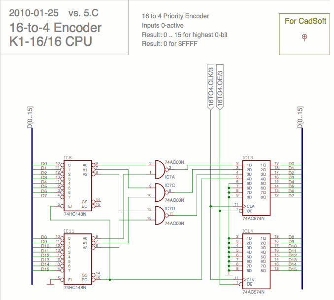
The 16-to-4 encoder is primarily used to determine (one of) the pending interrupts: When starting interrupt handling the CPU reads the interrupt state of all attached boards, which signal their state on "their" data line. The CPU then has to pick (one of) the pending interrupts. For this it could shift the 'interrupt pending' result word until it finds a 0-bit, but the 16-to-4 decoder will hopefully speed-up this task.
For the sake of hardware simplicity and because this matches the 0-active interrupt state, the input word is scrutinized for the most significant '0' (zero) bit. I don't know whether active-high 8-to-3 decoders were ever built.
The result for $FFFE (LSB = 0) and $FFFF (no 0-bit at all) is 0 in both cases. This can be distinguished by testing the word in the ALU, which can be done without actually loading it into the ALU, only the option control lines must be set appropriately.
The Box "For CadSoft" is for CadSoft only. Eventually they'll fix it.
The random bit generator consists of a zener avalanche break-through noise generator mixed with a 19 bit pseudo random shift register. The noise signal was not good enough to be used directly as a true random source, therefore i mix it with the shift register signal. The result bit is output to feedback line 'RND', previously used for the now obsolete ALU.Z88 feedback signal. To read a 16 bit random value you have to shift in 16 of those bits, which takes 16 clock cycles.
I have favoured the sparce resource of a feedback line over a plain vanilla data bus unit, because this reduced the head count on the PCB dramatically. Especially because of reusing the sensor ring shift registers and 4 data registers from the 74AC164 which also supplies two registers for the reset circuit. The 2 XOR gates come from the same IC which is used to pump the voltage which is required for the noise source. So overall well used resources. :-) Still, the used resources may not be worth the benefit of a real RNG. But this thing has cost me so such time and effort, that it had to go on the board.
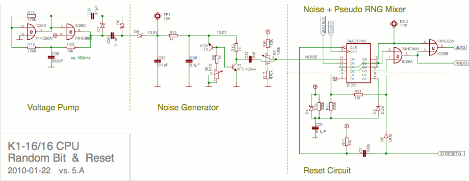
Two XOR gates are wired up to form an astable multivibrator which drives a voltage pump for approx. 13.5V @ 3.5mA. This is regulated to approx. 10V by a current sink which is built around a reverse connected BC556 transistor, a better zener diode, which i have selected to break through at approx. 9.5V. The break-through current drives the following amplification transistor, which regulates the voltage by drawing current until there is no longer enough voltage left to break through the noise source and which amplifies the noise AC signal, which is decoupled and centered and fed into the input of a data register of the 74AC174. Here it is synchronized with the main CPU clock (whick clocks the data registers), so that the output signal can only toggle once per clock cycle.
The two first 74HC166 shift registers from the sensor ring (see below) are also used as the first 16 bit of a pseudo random number generator shift register. Three data registers from the 74AC174 are used to form 3 more stages. I need access to the last and the 3rd-last stage, which are XORed and fed into the first stage of the shift register, which is a common pseudo RNG setup. These stages should have no common denominator. So i have choosen the output of stage 17 and 19. (15+17, which is more common, was not possible, because i have no access to the output of stage 7 (for stage 15) inside a 74HC166 shift register.)
The result of the XOR is not used directly, as for a pure pseudo RNG, but again XORed with the noise signal. If you XOR a real random signal with any useful data the result is real random again. So, if one of both is real random, XORing won't hurt. Here both sources have their limitation: The shift register delivers no real random and the noise signal's upper frequency is not high enough for one independent bit per CPU cycle, but mixing them eliminates their respective drawbacks. Off course therefore the result is no ideal random signal too, but pretty close to that.
The reset circuit is my 3rd try. I hate this analogous stuff. Try 1 malfunctions on the control unit board. Try 2, based on a 74HC423 monostable flip-flop, which i have plenty in stock and no use for, promised to trigger on power-up too but didn't. So here is try 3:
After reset capacitor C31 is empty and slowly fills up. As a result the input to data register D2 is low, this is clocked by the main CPU clock into the register and the output pulls !Reset low. When C31 fills up the input to the data register reaches '1'-level and – synchronized by the main CPU clock – the reset is released. The 1M resistor feed-back is used to make the register's input a Schmitt-Trigger.
If a remote source pulls !Reset low again, this also pulls the !CLR input of the 74AC174 low for a short time, because the signal runs through a small capacitor. This makes the output of the data register D1 go low immediately, which discharges the timing capacitor C31, and the output of D2 too, which now in return pulls !Reset low, even if the remote source goes away. After the !CLR signal fades away, the next main CPU clock pulse loads '1' into D1 which no longer discharges the timing capacitor. After the timing capacitor fills up, the '1'-state is copied – synchronized by the main CPU clock – into D2 which no longer pulls !Reset low.
SO, this circuit performs three tasks: Power-up reset, elongate short (but not too short :-/) reset pulses and release the reset signal synchronized with the main clock. It does not handle the software reset on the control unit, which i have to fix somehow too.
2010-01-13: 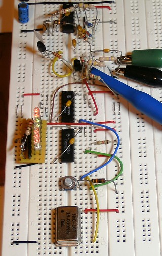 To the right the noise generator on the breadboard: At top is the voltage pump, driven by an oszillator built from 2 XOR gates running at 150kHz approx., next on the left side comes the noise source, a BC556 with an emitter – base break-through voltage of approx. 9.5V (the transistor with the paper flap), the garbage around the probe is the 1-transistor amplifier stage, the output runs into a 74AC174 data register, which is clocked by the 16 MHz quartz oven in front to mimic the planned circuit on the I/O board, the output of the 74AC174 is fed into a 74HC595 shift register, which is also clocked by the 16MHz signal and which outputs are displayed on the LED panel to the left.
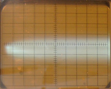
Noise signal at dx=100ns/cm and dy=0.8V/cm
Among others, the 'new front panel' will be able to display the state of all bus lines. For this, all bus lines are connected to a huge ring of shift registers. There are 96 bus lines in total, 16 data, 16 address lines, 2*16 data bus control and 2*8 address bus control lines, and 16 'other' control lines, including feedback and option control lines.
Therefore 12 74HC166 8 bit shift registers are required in total. The ring (ok, obviously no 'ring') starts at the 'other' lines, runs through the control bus, the data bus and the address bus and finally into the sensor ring connector. This connector carries a clock line SCLK, a data latch strobe !SLD and the serial data output SDO.
The front panel can freeze the CPU and single-step the main CPU clock in half-cycles. At any time it can load the state of all bus lines and then shift and read them slowly-but-shurely in order to display or scrutinize them.
The current design imposes some side effects which must be cared for:
The first two shift registers are also used for the first 16 bit of the pseudo random shift register for the random bit generator. The 74HC166 shift registers have two clock inputs which are attached to the frontpanel's clock SCLK and the main CPU clock CLK. One clock must be low in order for the other to be used. So under normal operating conditions SCLK must be held low in order for the RNG to work. Therefore this input has a pull-down resistor, in case the frontpanel is not attached. Then these 16 bits are shifted with every cycle of the main CPU clock, and the output of bit 16 – the output of the 2nd shift register – is mangled and mixed with the hardware noise signal and fed back to the input of bit 0, the input to the 1st shift register, or on a larger scale, the input to the whole sensor ring.
If the CPU is halted by the front panel, the main CPU clock is frozen. The front panel should halt the CPU in the 2nd half of a main clock cycle, when the main CPU clock is low. Now it can latch the state of all bus lines into the shift registers with a pulse on !SLD and then shift them all in by clocking SCLK. After that the CPU clock can be released while the frontpanel displays the state on it's LCD.
There are some 'mixed mode' options:
The frontpanel may be programmed to start tracing at a certain program address. Therefore the ring is organized so that the address bus state is shifted out first. The front panel can single step the CPU and in each cycle check the address by reading in (parts of) the address only, until it matches. This way the drag-down of the CPU is reduced, compared to reading the whole thing.
The frontpanel may release the CPU main clock after only shifting in the first 16 bit and continue shifting in the remainder while the CPU is running. This way the drag-down for the CPU running in 'showroom mode' is reduced. Drawback is that the random bit generator now probably generates bits of reduced quality, because the shared registers are clocked from two sources.
Basically it is also possible to read the bus state in the 1st period of a main CPU clock cycle. Then only the 16 bit from the shared shift registers can only be retrieved after advancing the main CPU clock one half-cycle into the 'low' phase. But this state is of low interest anyway, because it only differs in the data bus and address bus read clocks *.clk which are activated in the 2nd half of the clock cycle only. All other signals are (or should not) be affected by the main CPU clock state.
The frontpanel can read the 16 bits for the random number generator from the shared registers. If it resumes reading it will effectively read the bit from the noise source, because the shifting of the last 3 stages of the PRNG is inhibited as they are only clocked by the CPU clock itself. (see random bit generator circuit above.) The quality of the noise source could be validated this way, but it is probably better to do this with a program running on the CPU itself, because the front panel clock is much slower than the CPU's onboard clock.
To summarize: The sensor ring enables the frontpanel to display state info, or set a break point and trace a program. The inner state of the CPU's control unit or the contents of registers and ram cannot be retrieved this way.
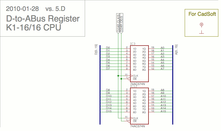
This register is the 'final addition' to the I/O board and the whole CPU. It is a register with inputs connected to the data bus and outputs connected to the address bus. It is intended for addressing global data, when the address is read from ram, e.g. via (PC++) as an immediate argument to an instruction, and immediately used for addressing data without offset. Without this register the microcode would have needed to load the address into a scratch data register and then load it into a scratch address register across the D2A bus bridge, before it can be used for addressing the ram. It will also save me the usage of these two scratch registers.
| Name | Letzte Änderung | Länge | |||
|---|---|---|---|---|---|
| Images/ | 2019-08-20 05:21 | 10 | |||
| 74148.HC.pdf | 2007-07-09 14:41 | 82850 | |||
| 74166.AC.pdf | 2008-02-10 19:54 | 73322 | |||
|
circuit 16-to-4.png size: 678 × 608 |
2010-01-30 18:44 | 29218 | ||
|
circuit d2ar.png size: 768 × 456 |
2010-01-30 18:44 | 20068 | ||
|
circuit io.png size: 694 × 621 |
2010-01-30 18:43 | 43047 | ||
|
circuit rnd+reset.png size: 920 × 356 |
2010-01-30 18:44 | 29488 | ||
|
circuit sensor ring.png size: 920 × 544 |
2010-01-30 18:44 | 68166 | ||
| Component Placing.pdf | 2010-02-20 16:11 | 87988 | |||
| K1-Bus 5.E.b#1 | 2010-02-20 16:15 | 140088 | |||
| K1-Bus 5.E.b#2 | 2010-02-20 16:10 | 140040 | |||
| K1-Bus 5.E.b#3 | 2010-01-31 12:24 | 139272 | |||
| K1-Bus 5.E.brd | 2010-02-20 18:23 | 140088 | |||
| K1-Bus 5.E.pdf | 2010-01-30 18:40 | 74629 | |||
| K1-Bus 5.E.s#1 | 2010-01-30 18:21 | 247518 | |||
| K1-Bus 5.E.sch | 2010-02-20 18:22 | 247518 | |||
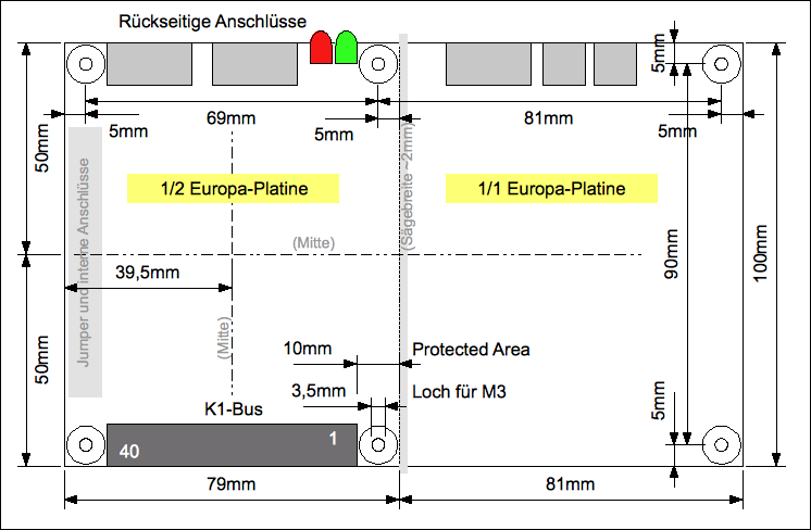 |
K1-Bus Board Dimensions.png size: 746 × 488 |
2008-12-24 13:47 | 48806 | ||
 |
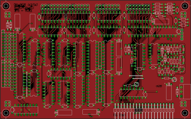
K1-Bus Board Layout.png size: 644 × 401 |
2009-10-05 20:06 | 16159 | ||
| K1-Bus.txt | 2010-01-23 00:30 | 1613 | |||
| Part List.txt | 2010-02-20 16:17 | 2686 | |||
| rnd.vs | 2017-07-04 21:25 | 262 | |||
| signal lengths.txt | 2010-01-29 18:14 | 130 |
powered by vipsi - your friendly VIP Script Interpreter
![]()
![]()