
|
k1.spdns.de / Develop / Hardware / K1-Computer / K1-CPU / |
 Start
| Overview
| Control Unit
| Microcode Header
| Arithmetic Unit
| Data Registers
| Address Registers
| Expansion Bus Start
| Overview
| Control Unit
| Microcode Header
| Arithmetic Unit
| Data Registers
| Address Registers
| Expansion Bus
|
|
|
k1.spdns.de / Develop / Hardware / K1-Computer / K1-CPU / |
| Start
| Overview
| Control Unit
| Microcode Header
| Arithmetic Unit
| Data Registers
| Address Registers
| Expansion Bus
|
Last updated: 2014-08-16
Questions & comments to Kio
The K1-16/16 CPU is the heart of the self-designed and home-built K1-16/16 Computer.
It is built with CMOS ICs from the 74AC series and fits on 5 Euro boards (160 x 100 mm).
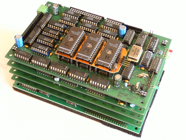
The CPU consists of 5 printed circuit boards. Internally it has a separated 16 bit data bus and a 16 bit address bus. All functions and data transfers are controlled by the control bus.
The control bus consists of control lines to control data movement between 16 units on the data bus and 8 units on the address bus. Additionally there are 4 option control lines for data bus units and 2 option control lines for address bus units. There are 6 feed-back lines, which are roughly the same as flags, except that they are not stored in a flag register. All control lines originate from the control unit, except for the feed-back lines which end here.
The control unit contains microcode roms, which are programmed to implement the machine code words. The microcode is loaded from eproms into fast rams during system reset.
The CPU also contains 64k of 16 bit internal RAM. The ram can be read and written in one clock cycle. The CPU does not have circuitry to connect external ram, but an external ram card might be attached to the K1-Bus.
The I/O board connects the CPU to the 16 bit K1-Bus, a universal peripheral bus. Up to 16 units can be attached to the K1-Bus with individual priorizable interrupts. The K1-Bus also attaches an i2c bus for code & data eeproms.
 In every cycle of the main clock CLK the CPU performs one data transfer on the data bus and one transfer on the address bus. At any time one data bus unit puts it's data on the data bus and one address bus unit puts it's address on the address bus. Switching between data sources is done without any gap, which results in short collisions during transition. Therefore all outputs to the data bus must be of the same circuit family. Same applies for the address bus.
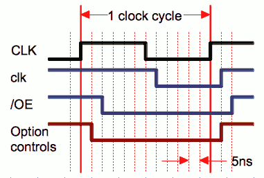
The data bus control consists of 16 x 2 control lines for 16 units attached to the data bus: 16 write signals 'clk' and 16 output enables '/OE'. A 'unit' may be a register or a function block; e.g. the whole ALU is a single function block on the data bus.
In every clock cycle of the main clock 'CLK' one data transfer is performed on the data bus. Exactly one unit is selected to put it's data on the data bus and exactly one unit is activated to load this data.
The output enables '/OE' are active-low. At any time one unit is activated to put it's data on the data bus. Switching between units is performed without gap. This implies a short bus collision while switching data sources which i tried to minimize by 'signal shaping' with low pullup resistors. (see control unit for details.)
The data write signals are named 'clk' because they are connected to the 'clk' input of edge-triggered data latches, 74AC574 in most cases. The clk signal is high in the first half of a bus cycle and goes low for the selected unit in the second half. The data is latched at the rising edge of the clk signal. The clk signals are 'strobed' with the system's main clock CLK. The resulting timing is that the active clk edge rises shortly before the /OE signals change for the next bus cycle.
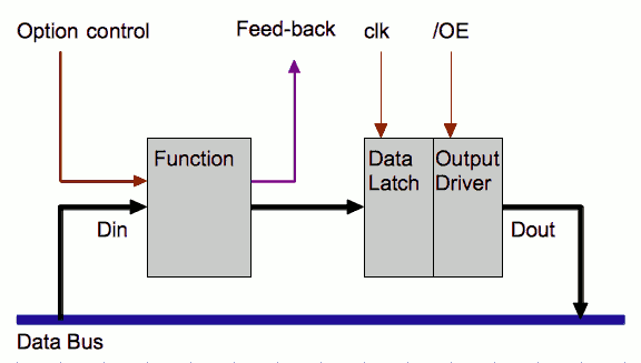 If the target is a function unit, then the function is performed on the data read from the data bus at the time of reading. At the end of the cycle the result is latched into the function's data register and can be put on the data bus in the next clock cycle.
A major drawback of this design is an increased power consumption and RF emission, because all function units permanently perform their function on the data currently present on the data bus, whether they are the choosen one to actually load the data or not. I have choosen this design over the 'apply function on output data' design because in my design the data latch preceeds the output driver stage directly and so they can be combined in a 74AC574 IC. In the other design the 'function' would be located between data storage and output driver and therefore they would need to go into separate ICs.
The address bus control consists of 8 x 2 control lines for 8 units attached to the address bus: 8 write signals 'clk' and 8 output enables '/OE'. Most 'units' are registers.
Output enables '/OE' and write clocks 'clk' work as for the data bus.
In every clock cycle of the main clock one data transfer is performed on the address bus. Exactly one unit is selected to put it's data on the address bus and exactly one unit is activated to load this data. The major destination for these addresses is the built-in ram, but it is never explicitely selected. When a data transfer on the data bus uses the ram, then the address currently visible on the address bus is used. Therefore often the address bus destination must be a 'dummy' data sink.
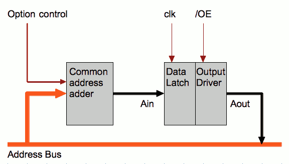 The inputs of the address registers are not connected to the address bus directly – instead they are connected to the output of a common address adder, which performs the functions +1, -1, +IVAL or +IVAL-256 on it. An address register cannot be loaded into another address register without adding an offset! (Data registers can be loaded into address register with offset ±0.) IVAL is the low byte of the current instruction code.
All CPU boards have a common design for vertical busses and screw holes. The boards can be stacked in any order, though the control unit should go on top, because the microcode eproms are located above the microcode rams, thus the control unit is thicker; and an easy access to the eproms is probably desirable.
The board template is defined in the EagleCad symbol library K1-Bus.lbr which also contains templates for K1-Bus peripheral cards.
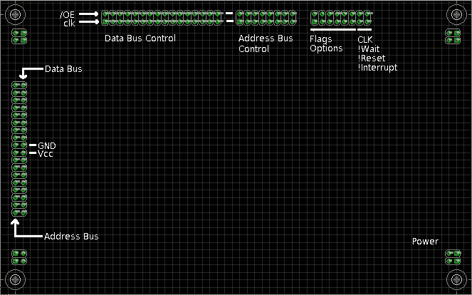
Common CPU board layout
Screw holes are 5mm from each corner and for M3 (3mm) screws.
In the corners are power connectors, square pads are GND and octal pads are +5V.
The left-side socket provides the data & address bus. The outer pins are the address bus, the inner pins are the data bus. Top pins are pins A0/D0 and bottom pins are pins A15/D15. In the middle are 4 additional power pins.
At the top is the control bus. It is split into data bus control, address bus control and other controls.
The data bus control consists of 2 control lines each for 16 units attached to the data bus: A write signal 'clk' and a output enable '/OE'. A 'unit' may be a register or a function block; e.g. the whole ALU is a single function block on the data bus.
from left to right
0: CMD   - control unit: clk loads next instruction; /OE puts immediate data on the bus
1: MEM   - the built-in ram
2: IO    - expansion bus
3: A2D   - address-to-data bus bridge: /OE puts the data from the address bus on the data bus
4: D0    - data register D0
5: D1    - data register D1
6: D2    - data register D2
7: D3    - data register D3
8: ALU   - Arithmetic/Logic Unit; incorporates a register as well
9: xxx   - not used
10 SWAP  - function: swap high byte and low byte
11 xxx   - not used
12 SR    - function: shift right
13 SL    - function: shift left
14 16to4 - function: 16-to-4 priority encoder
15 IVAL  - immediate value: low byte from the current instruction code
The middle block of the control bus is for the address bus controls.
from left to right
0: PC  - program counter: program execution address
1: D2A - data-to-address bus bridge: /OE puts the data from the data bus on the address bus
2: SP  - stack pointer
3: A0  - address register A0
4: A1  - address register A1
5: A2  - address register A2
6: A3  - address register A3
7: xxx - not used / dummy data sink
Other controls are 6 option control lines, 6 feed-back lines (flags) and 4 basic signals.
The inner left 6 lines on the right block are option control lines. They are used to 'modify' the function of function units. 4 lines are dedicated to data bus units, 2 to the address adder.
from left to right
OPT.FU0 - function selector for the ALU: LOAD, ADD, XOR, AND|OR
OPT.FU1 - ""
OPT.CY  - carry input to the ALU adder and to the shift registers
OPT.CPL - inverter control for ALU data input (mostly used for subtraction)
A.CPL   - inverter control for address bus adder (for -1 and negative IVAL offsets)
A.ADD   - displacement selector for address bus adder: add 1 or IVAL
4 option control lines modify data bus function units and 2 modify the address bus adder. Basically, all 4 data bus option lines can also be used by any other data bus unit, because they modify the function when loading the data, and only one unit can load the data from the bus in each cycle. (The I/O unit uses the control lines to select between 6 possible i/o cycle types and for i2c bus control. This includes input cycles, which violates the scope of these controls but simplifies i/o in general.)
The outer left 6 lines on the right block are feed-back lines. The state of these lines can be used to fork microcode execution into one of the two code planes to implement conditional branching.
The ALU generates most of the feed-back lines: unsigned overflow carry, signed overflow, and zero. Two feedback lines are the data bits D0 and D15.
From left to right
CY   - unsigned carry output from the ALU
Z    - Zero output from the ALU
RND  - random bit from the random bit generator on the I/O board
OVFL - signed overflow output from the ALU
D0   - data bus bit D0; e.g. for carry output of the SR function
D15  - data bus bit D15; e.g. for carry output of the SL function
The 4 rightmost lines on the control bus are !Reset, !Interrupt, !Wait and CLK.
!Reset !Wait
!Irpt  CLK
• !Reset - reset: open drain input/output line.
• !Irpt - combined interrupt request from the I/O bus.
• !Wait - wait input from the I/O bus.
• CLK - main system clock.
| Name | Letzte Änderung | Länge | |||
|---|---|---|---|---|---|
| ALU/ | 2019-08-20 05:21 | 16 | |||
| ARegs/ | 2019-08-20 05:21 | 12 | |||
| DRegs/ | 2019-08-20 05:21 | 14 | |||
| IO/ | 2019-08-22 19:20 | 25 | |||
| Microcode Upload Header/ | 2019-08-22 19:20 | 12 | |||
| More…/ | 2019-08-20 05:21 | 3 | |||
| SSW/ | 2019-08-22 19:20 | 20 | |||
| K1-Bus.lbr | 2014-08-21 17:26 | 428656 | |||
| K1-CPU.brd | 2009-10-12 20:04 | 20182 | |||
| K1-CPU.sch | 2010-01-28 20:46 | 23392 |
powered by vipsi - your friendly VIP Script Interpreter
![]()
![]()