
|
/Develop/Hardware/K1-Bus Z80 CPU board with SRAM/ |
| k1.spdns.de / Develop / Hardware / K1-Bus Z80 CPU board with SRAM / |
|
|
/Develop/Hardware/K1-Bus Z80 CPU board with SRAM/ |
| k1.spdns.de / Develop / Hardware / K1-Bus Z80 CPU board with SRAM / |
The system consists of a CMOS Z80 CPU running at 6 MHz, one 32kB SRAM and one 32kB EPROM or EEPROM. It has no I/O except connection to a K1-bus. The K1-Bus allows attachment of 16 bit peripherals. K1-bus card selection is restricted to D0 .. D7.
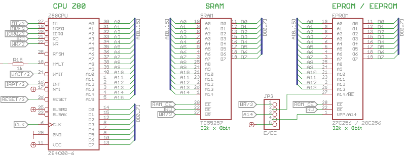
The Z80 uses separate instructions for I/O and memory access. Therefore the I/O address space is not part of the memory address space.
RAM is mapped to $0000 .. $7FFF and ROM is mapped to $8000 .. $FFFF. This allows modifying the RST vectors at run time.
After reset the ROM is mapped to the whole address space because the CPU starts execution at address $0000 and needs to find code there.
Pin header JP3 allows using an EPROM or an EEPROM. The EEPROM is writable by the Z80.
The RD and WR outputs of the CPU are directly connected to the RAM and ROM's corresponding inputs. Activation of the memory chips is done using their CE input.
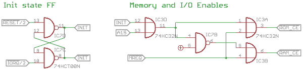
RAM is enabled when MREQ is low and A15 is low,
ROM is enabled when MREQ is low and A15 is high.
There is a 'init state FF' which is set by RESET and cleared by any I/O operation. Thus the FF is set after reset, will be cleared by the first I/O instruction and remain cleared throughout the rest of it's life. While it is set it forces A15 high in the RAM/ROM select circuit so that the CPU will always read from ROM.
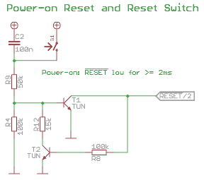 Reset circuit
The reset circuit was elaborated in great detail in my hardware blog. It is a little bit load dependent but should work up to 5mA pull-up current, which is much more than is to be expected, unless you attach a LED here. ;-)
With the selected value of the timing capacitor the reset pulse will be approx. 2 ms.
The CPU board does not contain any peripherals, not even a timer interrupt. All Peripherals are expected to be connected at the K1-bus.
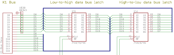
The K1-bus provides an I²C bus to attach EEPROMs with driver code and is 16 bit wide. Therefore two data latches are required for buffering data from the Z80's 8 bit bus to the upper half of the K1-bus.
I/O therefore is divided into I²C bus access, high-to-low and low-to-high data latch access and actual bus access.
The K1-bus is specified for symmetrical signals (HC, AC not HCT or TTL) therefore some signals may not have required levels without help.
K1-bus IRPT is directly connected to the IRPT input of the CPU. The interrupt source is determined in software.
K1-bus WAIT is directly connected to the WAIT input of the CPU. Any peripheral board which can issue WAIT fast enough can be used with this CPU board. Since the Z80 is pretty slow this probably means all peripheral boards.
The K1-bus address lines A0 to A5 are directly connected to the corresponding CPU address lines. They are pulled up with 3.3kΩ resistors to help the CPU to pull them up: The CPU has very little driving capabilities and driving high is even less than driving low:
IOL = 2.0mA     @0.4V
IOH = -1.6mA    @2.4V (which is too low for HC inputs)
IOH = -250µA    @4.2V
Eventually 4k7Ω is a better choice. To be tested.
The K1-bus data lines D0 to D7 are directly connected to the CPU as well, which is an allowed design for very small systems. Expect problems with the third card added! They are pulled up with 3.3kΩ resistors to help the CPU to pull them up for the same reason as above. The K1-bus data lines D8 to D15 don't need pull-ups because they are driven by the 74HCT574 which has symmetrical outputs (though TTL inputs) and slightly higher driving capabilities as well.
Any I/O instruction addresses the K1-bus. This is centered around a 74HCT138 3-to-8 decoder. It is enabled by IORQ=0 && M1=1. It then activates one of 8 strobe lines, depending on A6, A7 and WR. Pin headers JP4 allow to use A6, A7 and A8 instead and IORQ has a "strong" pull-up resistor. The reason for these circuit options are explained below.
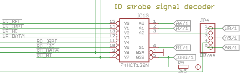
WR_SEL
Signal on the K1-bus to select a card for subsequent I/O operations. I/O cycles on the K1-bus do not contain the address of the talked-to card, instead a card must be 'selected'.
RD_IRPT
Signal on the K1-bus to read in the interrupt states of all cards to detect which one actually activates the IRPT line.
WR_IRPT
Signal on the K1-bus to mask off interrupts on some or all card. Can be used to implement interrupts with priority levels.
RD_DATA
Read data from a K1-bus card. The lower data byte is read by the CPU directly while the upper data byte (if present) is latched into the high-to-low data latch.
WR_DATA
Write data to a K1-bus card. The lower data byte is supplied by the CPU directly while the upper data byte (if required) is supplied by the low-to-high data latch.
WR_HI
Write one byte of data into the low-to-high data latch for use in the next (probably immediately following) WR_DATA cycle.
RD_HI
Read the upper data byte from the last RD_DATA cycle from the high-to-low data latch.
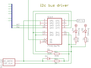 RD_I2C
Read or write to the I2C bus. Both is done by reading. The I2C data and I2C clock lines are set by A6 and A7, the value from the I2C data line is read on D7. The circuit is taken directly from my K1-bus page and was the only idea i had to use only one IC.
Errata: A6 and A7 cannot be used, because they are already in use to select the 74HC367! (They are used as select inputs to the strobe decoder.) Instead A3 and A4 are used.
The two LEDs are for debugging. It took me some time to find a place for some debugging lights on a CPU board without any i/o circuitry (except K1-bus) on it. :-)
A Z80 I/O bus cycle is strobed with IORQ by the CPU, so this is the first signal used to enable the signal decoder. But the CPU issues this signal for interrupt acknowledge cycles as well. This can be distinguished by the M1 signal, which is activated for interrupts but not for I/O cycles, so M1 must be high to detect an I/O cycle. M1 starts 2.5 cycles (that is: long) before IORQ and remains approx. 10ns longer active (M1: 80ns max. and IORQ 70ns max. after T3↑. These are marked with reference number 20 and 52 in the timing chart below) so it should be possible to use M1 directly to mask the IORQ signal.
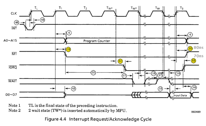
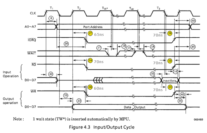
Next is a timing problem: WR (and RD) and IORQ go up simultaneously: 70ns max. after T3↓ as can be seen in the I/O timing chart below. This may result in spurious pulses at arbitrary outputs of the 74HCT138.
note: T3 in an I/O cycle is one cycle earlier than T3 in an int ack cycle: int ack inserts 2 automatic wait cycles before T3 and I/O only one.
There are some ideas to overcome this:
Besides WR (or A8, if nothing else works) A6 and A7 are chosen for strobe selection, because they are in the low address half, making all I/O instructions usable and they are the only unused address lines because A0 to A5 are already used for addressing K1-bus card registers.
| Name | Letzte Änderung | Länge | |||
|---|---|---|---|---|---|
| Data sheets/ | 2019-08-20 05:21 | 15 | |||
| Emulator/ | 2020-08-29 16:28 | 13 | |||
| Images/ | 2019-08-20 05:21 | 8 | |||
| V1.0/ | 2019-08-20 05:21 | 8 | |||
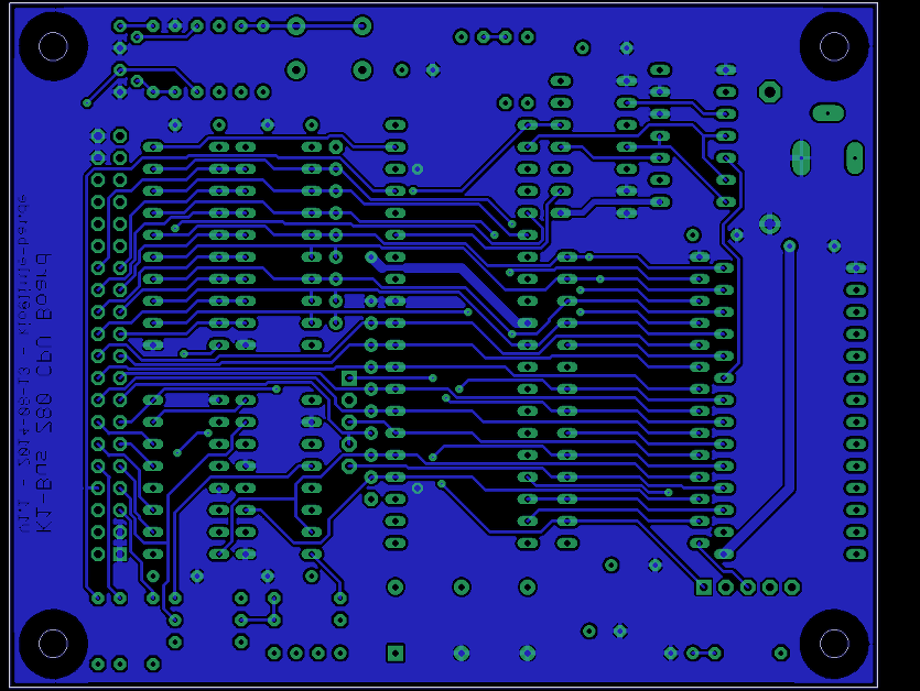 |
V1.1 board rear.png size: 835 × 628 |
2015-01-31 12:36 | 239161 | ||
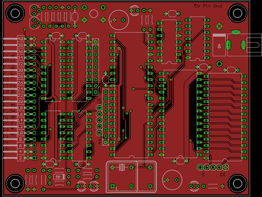 |
V1.1 board top.png size: 835 × 628 |
2015-01-31 12:35 | 314525 | ||
| V1.1 circuit io.pdf | 2015-01-31 12:25 | 82454 | |||
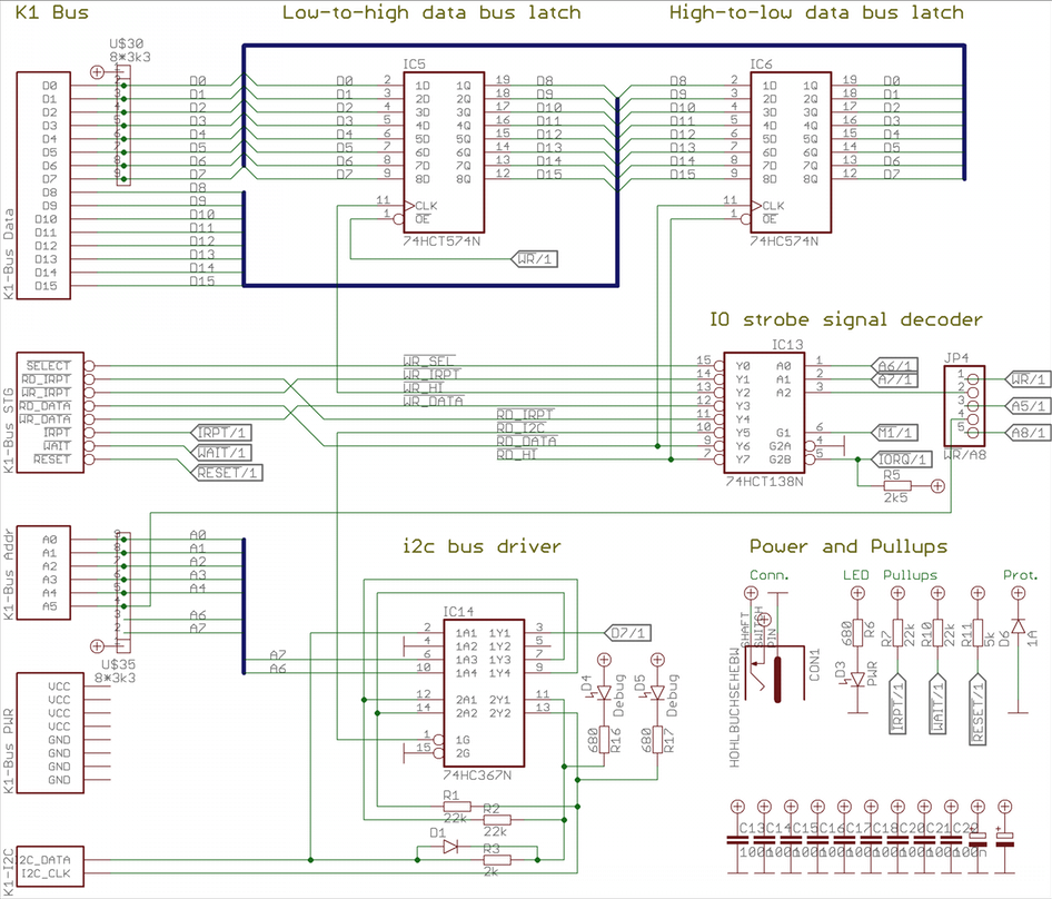 |
V1.1 circuit io.png size: 946 × 808 |
2015-01-31 12:39 | 293171 | ||
| V1.1 circuit main.pdf | 2015-01-31 12:24 | 96882 | |||
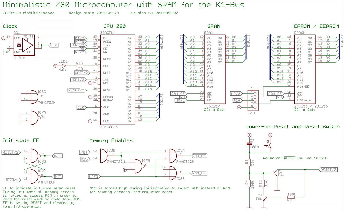 |
V1.1 circuit main.png size: 1191 × 732 |
2015-01-31 12:39 | 381993 | ||
| V1.1 part list.txt | 2014-11-09 15:43 | 2752 | |||
| V1.1 placement.pdf | 2014-11-09 15:34 | 47641 | |||
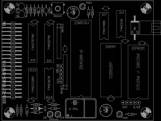 |
V1.1 placement.png size: 628 × 472 |
2014-11-09 15:33 | 14801 | ||
| V1.1.brd | 2015-01-31 12:11 | 185950 | |||
| V1.1.sch | 2015-01-31 16:54 | 397226 | |||
| V2.0.b#1 | 2016-04-03 12:34 | 186221 | |||
| V2.0.brd | 2016-04-04 20:36 | 186223 | |||
| V2.0.sch | 2015-06-23 20:48 | 397071 | |||
|
Z80 I:O cycle.png size: 693 × 445 |
2014-08-05 21:57 | 111670 | ||
|
Z80 Int Ack cycle.png size: 682 × 418 |
2014-08-05 21:57 | 101547 |
powered by vipsi - your friendly VIP Script Interpreter
![]()
![]()