
|
/Develop/Hardware/K1-Bus 68008 CPU board with SRAM/ |
| k1.spdns.de / Develop / Hardware / K1-Bus 68008 CPU board with SRAM / |
|
|
/Develop/Hardware/K1-Bus 68008 CPU board with SRAM/ |
| k1.spdns.de / Develop / Hardware / K1-Bus 68008 CPU board with SRAM / |
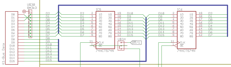
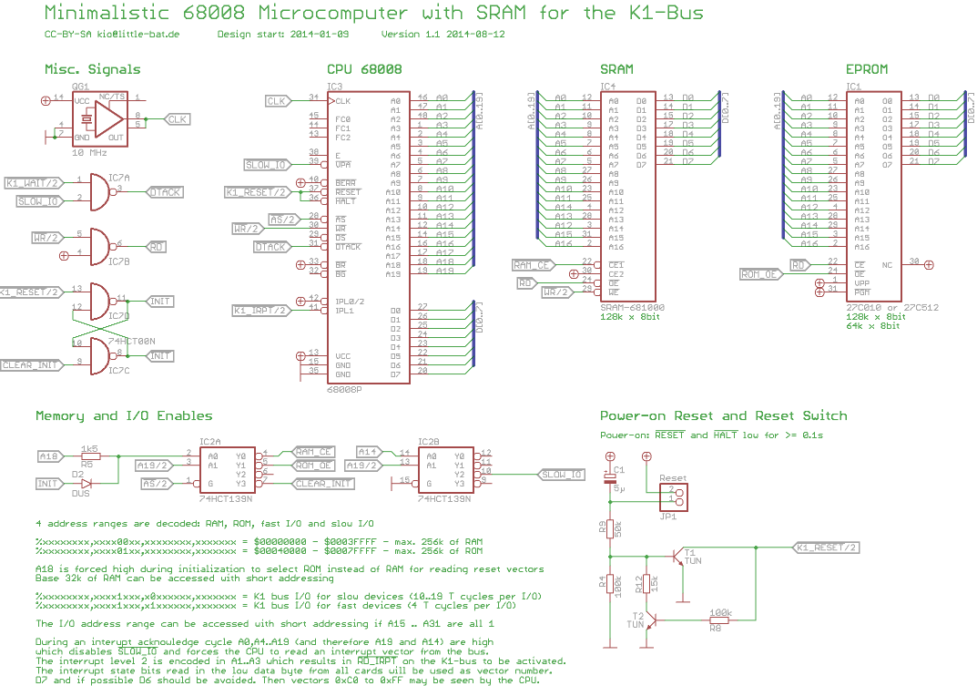
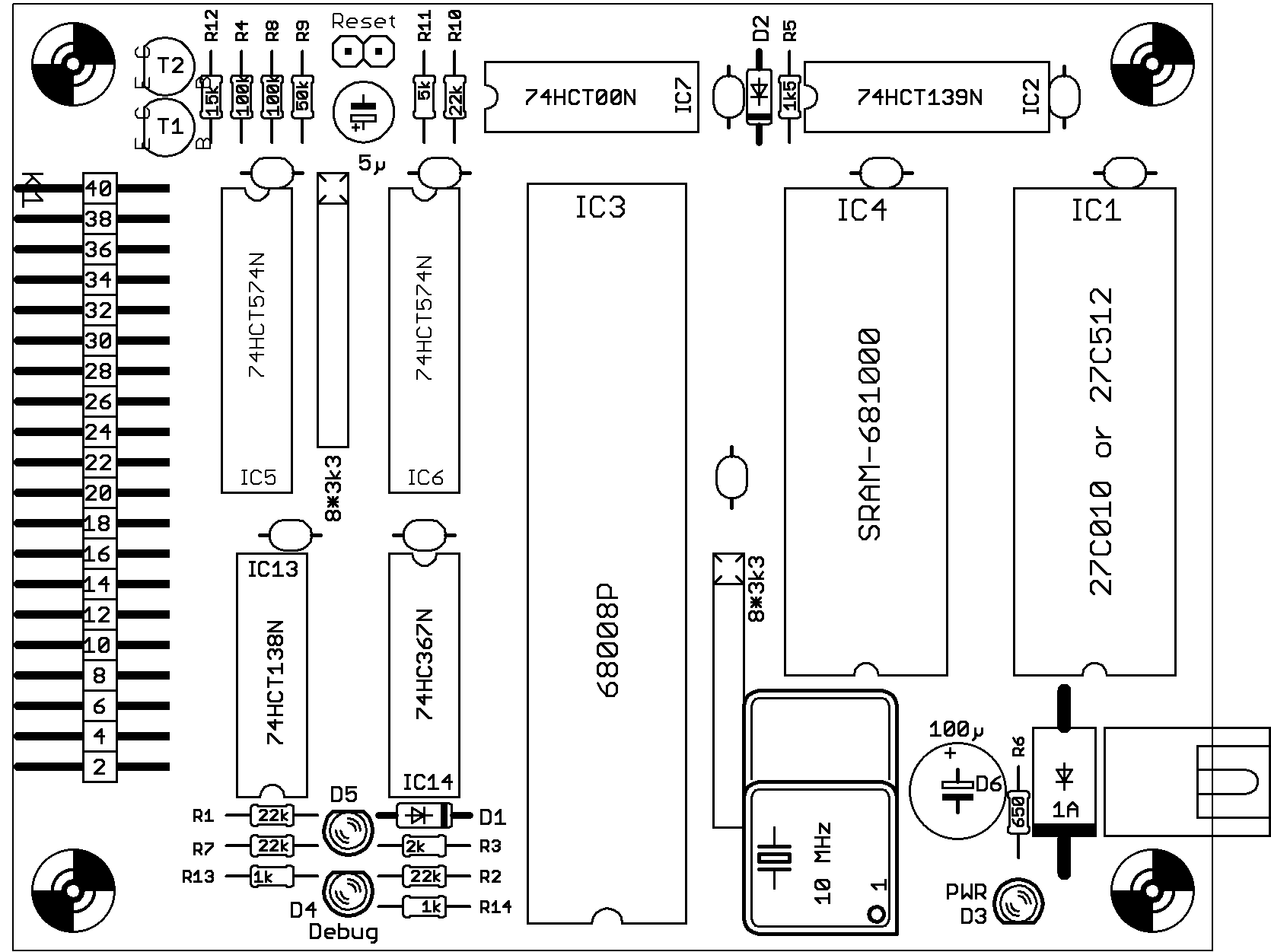
This is a simple 68008 CPU board for the K1-bus. It uses a 681000-70 128kB SRAM and one 27C010 128kB EPROM or one 27C512 64kB EPROM or similar. The board does not contain any i/o circuitry except for an unbuffered K1-bus. Even a system timer must be provided this way.
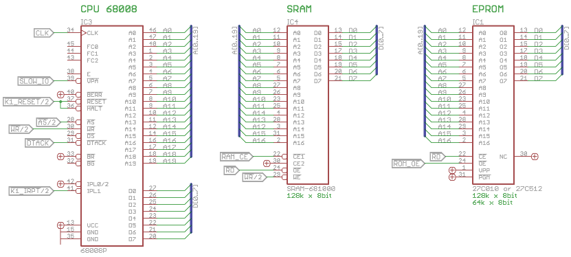
Main Circuit with CPU, RAM and ROM
The connection of RAM and ROM is very straight forward. Data bus lines and address bus lines are connected 1:1. Only two standard logic chips are used to interface the control signals: one 74HCT00 quad NAND and one 74HCT139 dual 2-to-4 decoder.
CPU control outputs used are /AS (controlling all bus cycles) and /WR (discriminating between read and write cycles). CPU control inputs used are /DTACK (terminate a bus cycle), /VPA (terminate a slow bus cycle) and /IPL1 (interrupt request).
CLK: a clock signal of 10 MHz is generated by a DIL clock generator.
FC0 to FC3: These outputs provide information about each bus cycle: Whether it's program or data and whether it's user mode or supervisor and whether it's an interrupt acknowledge cycle. I was thinking of using this to page-in ROM at address 0x000000 after reset but found it did not save me components and would make software more complicated. So these outputs are not used.
/BERR: signals a bus error to the CPU. Not used on this board. There will never be a bus error detected. All bus cycles terminate with /DTACK or /VPA.
/BR and /BG: Used for multi bus master control. Not used on this board. There is only one bus master: the CPU.
/RESET and /HALT: After power-up the CPU must be reset for 0.1 seconds (really!) by pulling these lines low. Both pins are outputs as well: /RESET can be asserted by software and will in return activate /HALT: this will halt the CPU after the current bus cycle, by when /RESET is already released again thus it should not cause problems to the CPU. Or /HALT can be asserted and will reset the CPU. /HALT is asserted if double bus errors are detected (and evtl. other conditions) and can eventually never happen with this board. To be tested when built :-) This signal is directly connected to the K1-bus /RESET line.
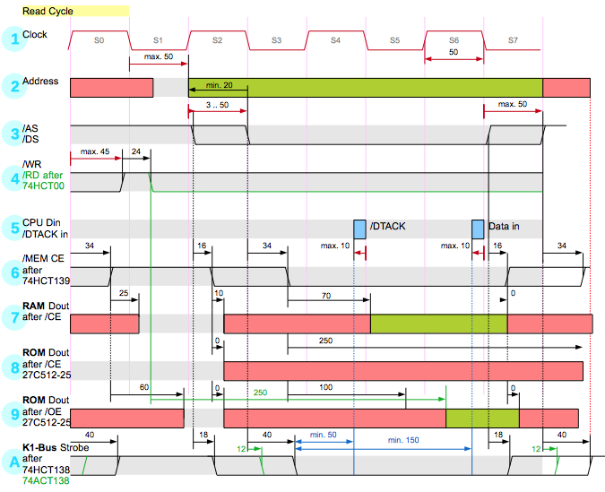
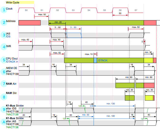
/AS: During a bus cycle /AS is activated while the address is valid. Basically /AS going low starts a bus cycle and /AS going high terminates it.
/DS is similar to /AS but in write cycles it is asserted slightly later than /AS. I thought that it was not asserted at all in 6800 cycles, because the signal is not shown in the 6800 timing chart, but it is, as can be seen in the autovector timing chart. This signal is not used.
/WR indicates that this bus cycle is a write cycle. The opposite signal /RD does not exist and is generated by an inverter.
/DTACK: Data Acknowledge is asserted by external circuitry to tell the CPU that it can finish the current bus cycle. It is possible to keep this signal low all the time so that the CPU will run without wait cycles. (Though the timing charts all tell you that this signal has to go up and down.) On this board /DTACK is asserted all the time except if /WAIT on the K1-bus is activated or a slow bus cycle is performed which will be terminated by /VPA.
/VPA is connected to a signal called /SLOW_IO: A bus cycle of the 68008 can be terminated normally in two ways: by /DTACK or by /VPA. /VPA means "valid peripheral address" and is used to interface old (very old!) 6800 peripherals. The 68008 then does an extremely slow bus cycle. I use this to do very slow i/o cycles on the K1-bus. /VPA has a second meaning: If an interrupt acknowledge cycle is terminated with /VPA, then the CPU does not read the interrupt vector from the data bus but generates an 'autovector' internally. This board does not use /VPA for interrupt acknowledge cycles. Instead it uses vectored interrupts and uses /DTACK to terminate interrupt acknowledge cycles.
IPL0/2 and IPL1: Interrupt inputs. The 68000 has 3 interrupt lines, the 68008 has only 2 due to pin shortage in the dip package and connects both IPL0 and IPL2 to one pin. Pulling low any combination of these lines forces an interrupt in the 68008. Pulling low all interrupt lines generates a non-maskable interrupt, pulling low less lines results in an interrupt of level 1 to 6. In the 68008 normal interrupts of level 2 (IPL1) and 5 (IPL0/2) can be generated. This board uses only interrupt IPL1, which is directly connected to the K1-bus interrupt line.
/CE: This enables the memory chip. While enabled, it can be read or written. The RAM also has a positive CE2 input, but this is not used. /CE is enabled by a 2-to-4 address decoder. See below.
/OE: If the memory chip is enabled, asserting /OE enables it's output drivers and the currently addressed byte is put on the data bus, where it can be read by the CPU. /OE is connected to the inverted /WR signal of the CPU: so at any time either /OE or /WR is enabled.
/WE: The RAM can also be written: if /WE is asserted while the RAM is enabled, then it will read the byte from the data bus and write it into the currently addressed memory cell. /WE is connected directly to the CPU's /WR output.
/CE and /OE of the EPROM are not connected as expected but swapped: the result is the same – the EPROM puts data on the data bus if both signals are enabled – but memory access after /CE is much slower than after /OE and enabling the chip with /CE would always require one wait state, at least if i use one of my (well stocked) 27C512-250 EPROMs with 250 nano seconds access time from /CE. But the EPROM's access time from /OE is only 100 ns, and therefore i connect /OE to the timing critical output of the 2-to-4 address decoder and /CE to the less timing critical /RD signal and can access the EPROM with no wait cycles.
Only two standard logic chips are used to interface the control signals: one 74HCT00 quad NAND and one 74HCT139 dual 2-to-4 decoder.
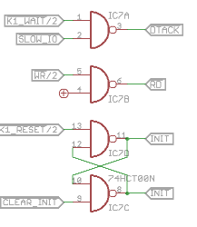 Bringing it all together
The 74HCT00 quad NAND provides one NAND, one inverter and one flip flop, as can be seen to the left.
The first gate generates /DTACK to terminate most bus cycles. /DTACK is permanently low except if /SLOW_IO or /K1_WAIT is low. /K1_WAIT originates from the K1-bus and /SLOW_IO is activated when access to a special address range is decoded.
The 2nd gate is used to invert the /WR signal of the CPU to generate the /RD signal required by the RAM and ROM.
Gate 3 and 4 construct a flip flop. After reset the CPU reads reset vectors from address 0x000000 which can only be provided by reading from ROM. But at runtime we'd like to have RAM at address 0x000000 to allow the running program to modify the vector table. To achieve this, this flip flop is set by the /RESET signal and cleared by the first access to an i/o address which activates signal /CLEAR_INIT. While set, the INIT output is used to temporarily map ROM at address 0x000000.
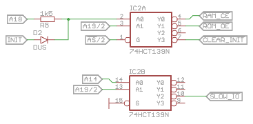 The two 2-to-4 decoders of the 74HCT139 are used to generate the RAM and ROM /CE signals, to clear the init_FF and to generate the /SLOW_IO signal.
The 1 MB address space of the 68008 CPU is divided into 4 regions: RAM, ROM, fast i/o and slow i/o.
The first decoder generates the RAM and ROM /CE signals. As explained above it actually generates /OE for the EPROM. For this it decodes the highest address lines A19 and A18: A19 must be low for both and A18 discriminates between RAM and ROM. This results in a memory map as follows:
0x000000 .. 0x03ffff  max. 256kB SRAM (actual size: 128kB)
0x040000 .. 0x07ffff  max. 256kB ROM  (actual size: 64kB or 128kB)
As explained above we need ROM at address 0x000000 after reset. Therefore signal INIT from the init_FF is used to pull A0 of the address decoder high, so that memory accesses in the RAM address range will activate the EPROM instead. Technically the resistor and the diode construct an OR gate.
The decoder is strobed with /AS from the CPU so that there are no spikes on the outputs when the address toggles between bus cycles. This is important, so that the RAM does not erroneously write some void data into random cells and that /CLEAR_INIT is not activated too early, e.g. immediately after reset before the CPU even read the first byte of the reset vector.
/CLEAR_INIT is generated when A19 is high and either A18 or INIT is high, and will clear the init_FF. A19 high means this is an i/o address.
The second decoder generates the /SLOW_IO signal, which is connected to the CPU's /VPA address input and to the first NAND gate to suppress /DTACK. If this signal is activated, the CPU will perform a very slow 6800 peripherals bus cycle. The signal is activated when A19 is high and A14 is low:
A19 must be high for any i/o access, because A19 low is used for memory access, either RAM or ROM.
A14 is used to discriminate between fast and slow i/o cycles. If we'd use A18 instead then the first decoder would have done the job. But A14 is used because it is in the low word of the address.
The 68000 uses 32 bit addresses but has a short addressing mode, where a 16 bit address is sign-extended to 32 bits. This saves program space and execution time, as only 2 address bytes must be read from memory.
If we want to use short addressing for i/o, then all address bits from A15 to A31 must be the same. And as A19 is high, they must all be high. (which besides means negative addresses for i/o). This makes A18 unusable for this task. On the other hand we cannot use A14 to discriminate between RAM and ROM as well, because that would break memory into 16 kB chunks. `:-)
Slow i/o is deliberately chosen to be activated when A14 is low:
When the CPU performs an interrupt acknowledge cycle, it puts the acknowledged interrupt level (which is always 2 on this board) on A1 to A3 and pulls all other address bits high. So during an interrupt acknowledge cycle A14 and A19 will be high and /SLOW_IO, and consequently /VPA at the CPU will not be activated and the CPU will do a fast bus cycle and will read a vector number from the data bus. This is explained in more details below.
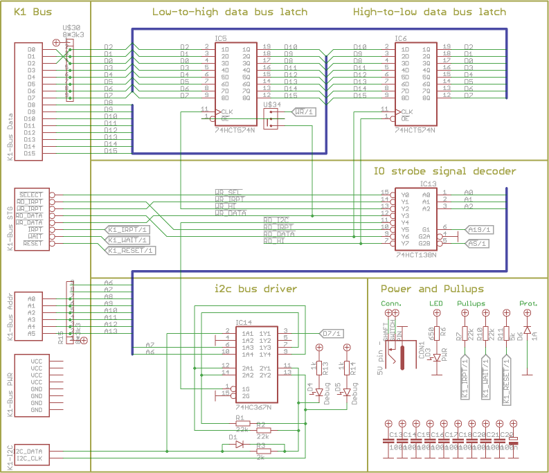
 This board uses a K1-bus for all peripherals. This is a hobbyist-grade 16-bit peripherals bus for CMOS devices which can be used unbuffered in small systems, as is done with this CPU board. The core K1-bus uses 16 data lines (8 may be sufficient for most cards), 6 address lines (4 mandatory) and 5 control lines, aka 'strobe lines'. It has one interrupt line, a wait request line and a reset line.
A unique feature of this bus is, that cards are not selected implicitly by the address in an i/o operation but must be selected beforehand instead. The address lines are only used to select registers inside the currently selected card.
Another unique feature of this bus is, that cards have an assigned data line which is used as their address. This data line is selectable with a jumpers on the i/o cards. This data line is used in conjunction with 3 of the strobe signals: /SELECT, /RD_IRPT and /WR_IRPT. The other 2 strobe signals /WR_DATA and /RD_DATA control data transfer to and from the card. This CPU board can only use data lines D0 to D6.
As can be seen in the circuit above, there are 3 more signals used: /RD_I2C accesses an I²C bus on the K1-bus, which is used to attach I²C EEPROMs which are used to detect cards automatically and which can provide driver code. Implementing the I²C bus interface is optional but recommended. /RD_HI and /WR_HI are used to control 2 data registers which pass data from the 8 bit data bus of the 68008 CPU to the high data byte of the 16-bit K1-bus. This is optional.
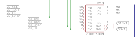
A 74HCT138 3-to-8 decoder is used to generate all these 8 strobe signals. A strobe signal is enabled when A19 is high, which on this board means an i/o access. A0 to A2 select which strobe signal to activate.
/AS is used to control output enable as well (to strobe the decoder outputs) so that strobe signals are only generated when the address is valid. Otherwise there would be spurious spikes on the strobe lines. The exact timing is tricky, due to wide timing windows in the 68008 timing charts, which i will discuss somewhere else.
There are 4 strobes for read cycles and 4 strobes for write cycles. They are assigned to the decoder so that using the CPU's /WR signal could have been used instead of A2. And originally it was. But the bus cycle timings for the 68000 are so lousy that the risk for spikes on the decoder outputs was too high and i decided to use A2 instead. Now the program must take care to access i/o addresses with bit A2 properly set, or there will be bus collisions when writing to a read address.
The /RD_IRPT strobe is connected to output number 5 to allow vectored interrupts:
The strobe signal decoder is also activated in an interrupt acknowledge cycle, because /AS is activated as in any bus cycle and A19 is high. A1 to A3 encode the acknowledged interrupt level, which is always 2 on this board.
So the address on the bus is %1……111110101, where the blue digits indicate the acknowledged interrupt level. So bits A0 to A2 are %101 which selects output number 5. This instructs all attached cards to put their interrupt state on their assigned data line: '1' if inactive and '0' if active. Additionally, the data bus has pull-up resistors (initially for helping the 68008 with pulling them up for the K1-bus) which will make all unconnected data bits read '1' as well.
So the vector read by the CPU is 0xff – x, where x is the active or potentially a combination of multiple active interrupts. If we never choose D7 for the assigned data line of a card, the vector will always be in range 0x80 to 0xFF, never conflicting with any other predefined vector. The vector table has to be filled with matching interrupt vectors. Wherever more than one bit is low in the vector address the program can decide which vector to store, e.g. always the vector of the interrupt with higher data bit number, thus implementing interrupt priorities.
The CPU's A0 is used for the strobe decoder's A0 to enable word write instructions. The 68008 first writes the high byte to the even address and then the low byte to the odd address. If writing to the right address, this automatically first stores the high byte in the low-to-high data bus latch and then writes both bytes in a 16-bit K1-bus /WR_DATA cycle. Unluckily the same magic does not work for read cycles: the word will be read byte-swapped and must be swapped programmatically, which is a little bit awkward, because the 68000 CPU has no opcode for this.
The low-to-high and the high-to-low data registers
Data is stored in the low-to-high data register when the /WR_HI strobe signal is active, which means, that the CPU writes to an appropriate i/o address, and it put's it's contents on the high byte of the data bus when /WR_DATA is active, while the CPU supplies the low byte.
There is a jumper option on the board to use /WR instead of /WR_DATA to enable the low-to-high latches outputs. This is to solve potential timing problems.
The high-to-low data register reads data from the high byte of the data bus when /RD_DATA is active while the CPU reads the low byte, and it put's it's contents on the low data bus when /RD_HI is active, which means, that the CPU is reading from an appropriate i/o address.
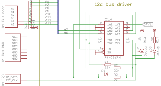 The I²C bus connection is centered around a 74HC367 2+4 bit driver IC. The circuit is described on my K1-bus page. A6 and A7 are chosen for data output to the I²C data and clock line. D7 is used to read the state of the I²C data line. All I²C signals and timings are generated by the CPU under pure software control.
The I²C bus is used to attach I²C EEPROMs which are used to automatically detect cards and which can provide driver code.
In addition, 2 LEDs are connected to the I²C driver for debugging the board. I spent some time to find a place to connect some lights, as this CPU board does not contain any i/o port pins.
A8 to A13 of the CPU are connected to A0 to A5 ot the K1-bus. Also, there are pull-up resistors on A7 to A13. This is because the 68008 CPU uses TTL levels for all signals and has only very poor high-driving capability, while the K1-bus is defined for symmetrical signals, as used by 74HCxx or 74ACxx series ICs.
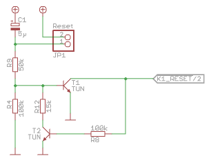 The reset circuit was already discussed in great detail in my hardware blog:
After power-up the capacitor is empty and current flows through it and through the base of transistor T1 which opens and pulls the /RESET line low. While /RESET is low T2 is closed. When C1 fills up the current decreases and at some point T1 does no longer drain all current from the /RESET line: the voltage rises and T2 will open and drain the remaining base current of T1 which will rapidly close: /RESET goes high and the system starts.
| Name | Letzte Änderung | Länge | |||
|---|---|---|---|---|---|
| 68000 Timing Diagrams/ | 2019-08-20 05:21 | 9 | |||
| Data sheets/ | 2019-08-20 05:21 | 12 | |||
| Images/ | 2019-08-20 05:21 | 5 | |||
| other people's 68008 projects/ | 2020-08-27 14:08 | 5 | |||
| Software 0.01 - first test program/ | 2020-08-29 18:09 | 10 | |||
| Super-Sinclair/ | 2019-08-20 05:21 | 3 | |||
| 68008 using DTACK.avi | 2014-01-23 16:44 | 2216252 | |||
| 68008 using VPA.avi | 2014-01-23 16:42 | 2515424 | |||
| eagle.epf | 2014-01-19 22:12 | 4908 | |||
| info_alt.vh | 2014-08-11 17:17 | 16268 | |||
| read cycle timing.odg | 2014-08-10 20:56 | 48670 | |||
 |
read cycle timing.png size: 675 × 549 |
2014-08-10 20:59 | 75183 | ||
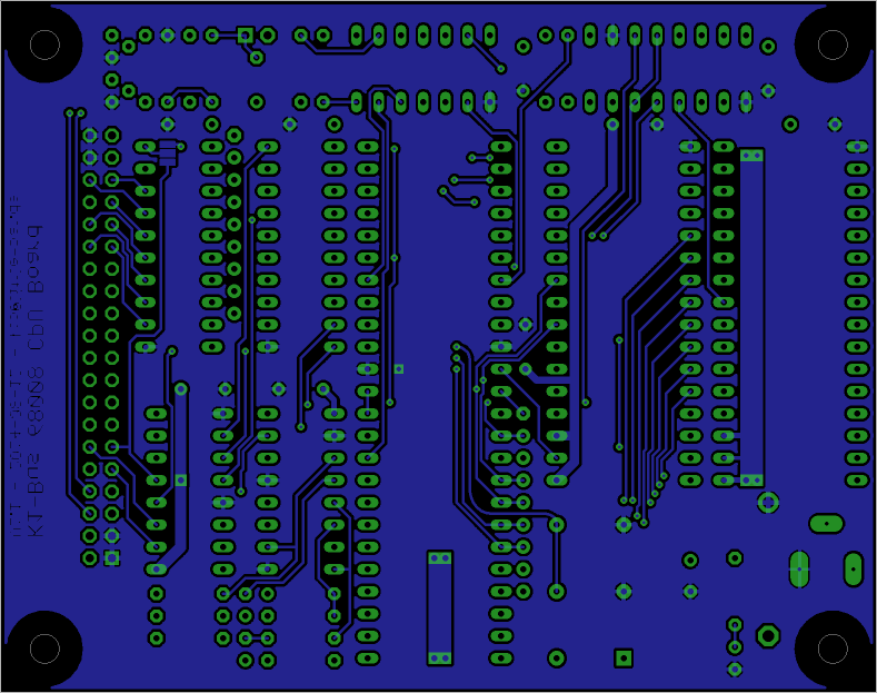 |
v1.1 board rear.png size: 789 × 623 |
2014-08-12 22:33 | 72125 | ||
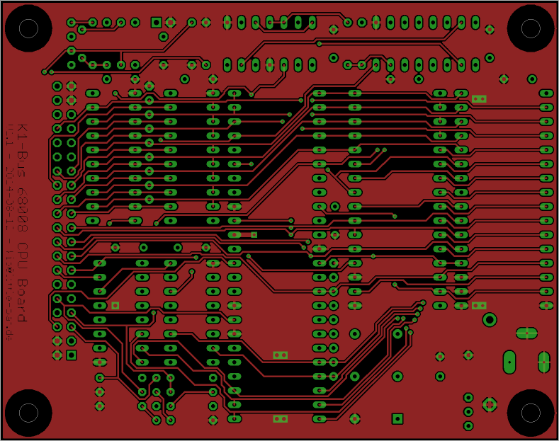 |
v1.1 board top.png size: 789 × 623 |
2014-08-12 22:31 | 70455 | ||
 |
v1.1 circuit io.png size: 793 × 683 |
2014-08-12 21:45 | 44936 | ||
 |
v1.1 circuit main.png size: 1073 × 753 |
2014-08-12 21:46 | 105110 | ||
| v1.1 part list.txt | 2014-11-09 15:50 | 2706 | |||
| v1.1 placement.pdf | 2014-11-09 15:45 | 45798 | |||
 |
v1.1 placement.png size: 1670 × 1251 |
2014-08-12 21:58 | 19992 | ||
| v1.1.b#1 | 2014-08-13 17:15 | 189651 | |||
| v1.1.brd | 2015-01-29 17:44 | 189652 | |||
| v1.1.s#1 | 2014-08-13 17:15 | 398182 | |||
| v1.1.sch | 2015-01-29 17:44 | 398198 | |||
| write cycle timing.odg | 2014-08-10 17:38 | 48341 | |||
 |
write cycle timing.png size: 674 × 547 |
2014-08-10 20:39 | 78020 |
powered by vipsi - your friendly VIP Script Interpreter
![]()
![]()