/*
this file is included by index.cgi
*/
var TITLE = «Simple 68008 Microcomputer with SRAM for the K1-Bus»
var DESCRIPTION = «One of my hardware projects: a simple 68008 Microcomputer with SRAM for the K1-Bus»
var KEYWORDS = «68008, 68000, 68k, M68k, K1-Bus»
var ROBOTS = «index,follow»
var MAIN = «
h2 Simple 68008 computer with K1-bus for i/o
p This is a simple 68008 CPU board for the K1-bus. It uses a 681000-70 128kB SRAM and one 27C010 128kB Eprom or one 27C512 64kB Eprom or similar. The board does not contain any i/o circuitry except for the K1-bus. Even a system timer must be provided this way. The board contains hi-to-low byte data registers to allow attachment of 16 bit i/o cards.
p The connection of ram and rom is very straight forward. The reset circuit was already discussed in great detail in my hardware blog.
p A 74HCT138 3-to-8 decoder is used to generate 8 control lines (strobe lines) for the K1-bus.
p The circuitry around the 74HC367 is used to read i2c EEproms on the K1-bus cards which contain driver code. Writing and reading to the i2c bus is done by reading. A6 and A7 control the clock and data line while the state of the data line is read back on D7. The circuit is taken quite verbatim from my K1-bus page.
p The 74HCT574 and 74HC574 are used to store the high byte for a data write cycle or to read the high byte from a data read cycle, if used.
p The usage of HC types (and not HCT types) here and there and some pull-up resistor networks are due to the K1-bus which uses symmetrical signals.
h2 Timing charts
p Before producing the PCB i reviewed the v1.0 design and found some problems and fixed them for v1.1. This way i also document most of the control lines and timings. :-)
h3 Low-to-high data latch !OE problem
p The 74HCT574 "low-to-high" data latch is used in a K1-bus write cycle to put the high byte on the data bus because the 68008 only has an 8-bit bus. It's output is enabled by the K1-bus strobe signal /WR_DATA. This means that data is valid only ~ 20ns after the strobe is going low. Most cards will work with this, but acc. to K1-bus specs data should be valid at least when the strobe goes low.
p I was thinking of fixing this by using !WR instead for output enable:
p Switch-on latency (min..typ..max):
pre /WR↓ = (5..25..45); 74HCT138 delay = (9..18..40)
/AS↓ = (3..28..50); 74HCT574 delay = (10..19..33)
/WR_DATA↓ = /AS↓ + 74HCT138 = (12..46..90)
data valid after /OE with /WR = /WR↓ + 74HCT574 = (15..44..78)
data valid after /OE with /WR_DATA = /WR_DATA↓ + 74HCT574 = (22..65..123)
p Data validity after /WR_DATA↓ is much better. It's even better, because there is a guaranteed max. delay of /WR behind /AS of 10ns in the 68008 timing chart. So worst case of data valid can't meet best case of /WR_DATA strobe. But it's not guaranteed.
p Switch-off latency:
pre /WR↑ = (55..75..95); 74HCT138 delay = (9..18..40)
/AS↑ = (5..28..50); 74HCT574 delay = (8..16..28)
/WR_DATA↑ = /AS↑ + 74HCT138 = (14..46..90)
data invalid after /OE with /WR = /WR↑ + 74HCT574 = (63..91..123)
data invalid after /OE with /WR_DATA = /WR_DATA↑ + 74HCT574 = (22..62..118)
p Data hold time after /WR_DATA↑ looks better but isn't: Using /RD_DATA guarantees ~16ns data hold time, while with /WR there typically is an even longer data hold time, but a chance for invalid data before /DR_DATA goes up. But we'll probably never see the combination of worst case + best case and data on the data bus remains valid for some more time, if noone else starts driving the bus.
p Conclusio
p Using /WR for /OE typically performs better, but still does not guarantee valid data immediately after /WR_DATA↓. And it does not guarantee valid data until /WR_DATA↑, while using /WR_DATA does. And, fun fact, see below, data on D0..D7 is not guaranteed to be valid immediately after /WR_DATA↓ as well. So the better choice is probably to stick with enabling output of the 74HCT574 data latch with /WR_DATA.
h3 Using !WR as an address input to the K1-bus strobe signal encoder may cause spikes
p The 74HCT138 3-to-8 decoder used to generate the K1-bus strobe signals used !WR as one of it's signal select inputs and !AS as one of it's output enable inputs. According to the 68008 write cycle timing chart !WR goes low up to 10ns after !AS (time #20A). This may result in spikes on arbitrary outputs of the 74HCT138.
p I thought i could fixed this by using !DS instead of !AS, which goes low one clock phase later (50ns @ 10MHz) in a write cycle. But due to timing problems discussed below, this was no option. As an alternative i can use an unused address line to discriminate between read and write cycles.
p pro & contra !DS + !RW:
+ also asserts that data D0..7 is valid when asserting the strobe signal
– 50ns shorter write cycles
– !DS is not asserted in a 6800 bus cycle: "slow" i/o cycles not possible!
+ => we could use !DTACK for interrupt acknowledge cycles as well
(assuming stable pullups on D0..D7, interrupts will jump to vector 255)
– round-trip time for !WAIT ~ 0ns: K1-bus !WAIT signal not usable!
p Especially all three "–" features in conjunction disqualify this option.
p pro & contra !AS + Ax:
– data D0..7 may be invalid for up to 40ns (see below) when asserting the strobe signal
+ "slow" 6800 bus cycles possible
+ we can still use !DTACK for interrupt acknowledge cycles if we like
(assuming stable pullups on D0..D7, interrupts will jump to vector 255)
+ round-trip time for !WAIT ≥ 50ns: K1-bus !WAIT signal usable
– data collision on the data bus possible if writing to an i/o read address; e.g. if program crashed
h3 Discussion of read cycle timing
p 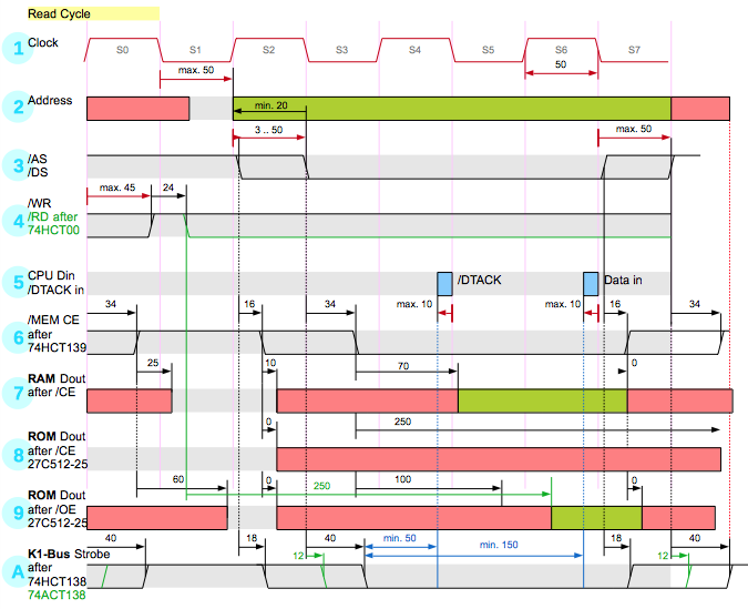 p Row (1) shows the 10MHz clock signal. One phase is 50ns long. (All times are expressed in ns.)
p Row (2) shows the 68008 address outputs. The address is valid ≤50ns after S1 but also guaranteed valid ≥20 before /AS and /DS go low, and guaranteed to 0ns after S0 of the next instruction. This will lead to timing problems. see below.
p Row (3) shows the /AS and /DS signals, which go up and down simultaneously in a read cycle. Actually used is the /AS signal due to the already discussed timing problem. /AS controls /RAM_CE, /ROM_CE and K1-Bus strobe enable.
p Row (4) shows the /WR signal and the /RD signal which is generated from /WR by an inverter (NAND gate). /WR remains high during a read cycle, but it may be low at the start of the cycle if the previous cycle was a write cycle. For this case this row shows the maximum latencies which are important for accessing the EPROM.
p Row (5) shows the short windows when !DTACK is sampled (for K1-bus !WAIT) and when the CPU actually reads the data byte from the data bus.
p Row (6) shows !RAM_CE and !ROM_CE generated from /AS (and non-critical from A18, A19) by one of the 74HCT139 2-to-4 decoder gates. "Typical" propagation time is 16ns and max. is 34ns. As /OE of the Ram and Eprom are connected to /RD which doesn't toggle in a read cycle, the /CE times determine the access memory time.
p Row (7) shows when the 681000-70 SRam drives data (red) and when data is actually valid (green). Even if looking at the worst cases this is totally safe within specs.
p Row (8) shows when the Eprom supplies valid data when controlled by /CE. This is after 250ns which means: Never. To fix this i swapped /CE and /OE. The reason is, that the /OE access time is only 100ns:
p Row (9) shows when the Eprom supplies valid data when controlled by /OE. In this case not the /OE access time of 100ns is critical but the /CE access time if the previous bus cycle was a write cycle. See the green reference lines. As in row 7 red color shows when the bus is (or may be) driven and green when data is valid. This is safely around the data read window of the CPU.
p Row (A) shows the timing for the K1-bus control lines (strobe lines). They are generated by the 74HCT138 and the timing is controlled solely by /AS, as all other inputs (enable G1 and 3 select inputs) are connected to address lines, which are stable at least 20ns before /AS at least stable 0ns after /AS.
In the worst case we have only 50ns for the i/o card to react with the !WAIT signal, which is OK and we'll probably never really see the worst timing case, 70ns are more likely the actual worst case. Cards which are too slow may still be used in "slow" 6800 mode.
In the worst case the card has to supply data within 150ns (170ns real world) if it doesn't assert !WAIT. Cards which are too slow may still be used in "slow" mode.
p Critical is the timing at the off-edge of the strobe signal: In the worst case it takes 40ns after S0 of the next bus cycle while the address is only guaranteed to be valid for 0ns. So the strobe signal decoder may activate a wrong control line for up to 40ns.
p The question is, how likely is this?
/AS will probably always go off faster than specified, because it only drives 2 inputs. Let's be optimistic and say this saves 20ns.
40ns for the 74HCT138 is also the worst case. "Typical" is 18ns. So save another 20ns.
20ns + 20ns = 40ns and we are done. :-)
p.red And if it fails?
p The address will almost certainly be also stable for at least 10ns, maybe 30ns after /AS goes off like the data lines, but we don't know that for sure. This adds another 10ns.
p.red And if it still fails?
p Then i'll use a 74ACT138 instead, which is much faster. (saving 25ns for the worst case.) I don't think i'll need it, but good to have it as a last resort.
h3 Discussion of write cycle timing
p
p Row (1) shows the 10MHz clock signal. One phase is 50ns long. (All times are expressed in ns.)
p Row (2) shows the 68008 address outputs. The address is valid ≤50ns after S1 but also guaranteed valid ≥20 before /AS and /DS go low, and guaranteed to 0ns after S0 of the next instruction. This will lead to timing problems. see below.
p Row (3) shows the /AS and /DS signals, which go up and down simultaneously in a read cycle. Actually used is the /AS signal due to the already discussed timing problem. /AS controls /RAM_CE, /ROM_CE and K1-Bus strobe enable.
p Row (4) shows the /WR signal and the /RD signal which is generated from /WR by an inverter (NAND gate). /WR remains high during a read cycle, but it may be low at the start of the cycle if the previous cycle was a write cycle. For this case this row shows the maximum latencies which are important for accessing the EPROM.
p Row (5) shows the short windows when !DTACK is sampled (for K1-bus !WAIT) and when the CPU actually reads the data byte from the data bus.
p Row (6) shows !RAM_CE and !ROM_CE generated from /AS (and non-critical from A18, A19) by one of the 74HCT139 2-to-4 decoder gates. "Typical" propagation time is 16ns and max. is 34ns. As /OE of the Ram and Eprom are connected to /RD which doesn't toggle in a read cycle, the /CE times determine the access memory time.
p Row (7) shows when the 681000-70 SRam drives data (red) and when data is actually valid (green). Even if looking at the worst cases this is totally safe within specs.
p Row (8) shows when the Eprom supplies valid data when controlled by /CE. This is after 250ns which means: Never. To fix this i swapped /CE and /OE. The reason is, that the /OE access time is only 100ns:
p Row (9) shows when the Eprom supplies valid data when controlled by /OE. In this case not the /OE access time of 100ns is critical but the /CE access time if the previous bus cycle was a write cycle. See the green reference lines. As in row 7 red color shows when the bus is (or may be) driven and green when data is valid. This is safely around the data read window of the CPU.
p Row (A) shows the timing for the K1-bus control lines (strobe lines). They are generated by the 74HCT138 and the timing is controlled solely by /AS, as all other inputs (enable G1 and 3 select inputs) are connected to address lines, which are stable at least 20ns before /AS at least stable 0ns after /AS.
In the worst case we have only 50ns for the i/o card to react with the !WAIT signal, which is OK and we'll probably never really see the worst timing case, 70ns are more likely the actual worst case. Cards which are too slow may still be used in "slow" 6800 mode.
In the worst case the card has to supply data within 150ns (170ns real world) if it doesn't assert !WAIT. Cards which are too slow may still be used in "slow" mode.
p Critical is the timing at the off-edge of the strobe signal: In the worst case it takes 40ns after S0 of the next bus cycle while the address is only guaranteed to be valid for 0ns. So the strobe signal decoder may activate a wrong control line for up to 40ns.
p The question is, how likely is this?
/AS will probably always go off faster than specified, because it only drives 2 inputs. Let's be optimistic and say this saves 20ns.
40ns for the 74HCT138 is also the worst case. "Typical" is 18ns. So save another 20ns.
20ns + 20ns = 40ns and we are done. :-)
p.red And if it fails?
p The address will almost certainly be also stable for at least 10ns, maybe 30ns after /AS goes off like the data lines, but we don't know that for sure. This adds another 10ns.
p.red And if it still fails?
p Then i'll use a 74ACT138 instead, which is much faster. (saving 25ns for the worst case.) I don't think i'll need it, but good to have it as a last resort.
h3 Discussion of write cycle timing
p 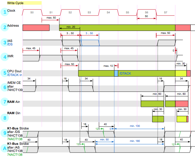 p Row (1) shows the 10MHz clock signal. One phase is 50ns long. (All times are expressed in ns.) (same as read cycle)
p Row (2) shows the 68008 address outputs. The address is valid ≤50ns after S1 but also guaranteed valid ≥20 before /AS, and guaranteed to 0ns after S0 of the next instruction. This will lead to timing problems. see below. (same as read cycle)
p Row (3) shows the /AS and /DS signals. /DS goes down one clock phase later than /AS. As discussed above i examined whether this could be used to fix some problems, but it couldn't and the /DS signal is not used. So only /AS is used which behaves same as in read cycles.
p Row (4) shows the /WR signal. It is output from the 68008 directly and no delay for a single gate is added as it was for the /RD signal. The /WR signal is only used to control writing data into the SRam. Due to timing problems it is not used to select K1-bus control signals, as discussed above.
p Row(5) shows the time when the CPU drives data to the data bus (green). Data becomes invalid 0ns after S0 of the next bus cycle, except, it is also guaranteed that it is valid at least 30ns after /AS goes up. In a worst case of /AS data may be valid for 30ns after S0 of the next bus cycle (yellow). As we'll see a K1-bus write cycle might even require 40ns (red).
Blue is the moment when the CPU latches /DTACK and by when !WAIT must be activated, if used.
p Row (6) shows !RAM_CE after the 74HCT139 2-to-4 decoder. (same as in read cycle) Critical timing input is from /AS and it adds it's varying delay to the varying delay of that signal. The on-edge is not critical, as the SRam latches data at the off-edge. The off-edge may happen anywhere from ~30ns before to 34ns after S0 of the next bus cycle.
p Row (7) shows when the 681000-70 SRAM requires the valid address. As can be seen in a worst case scenario for /AS and 74HCT139 we'll have an invalid address for up to 34ns (red) because the address is only guaranteed to be valid for up to 0ns after S0 of the next bus cycle.
p As said above we may hopefully not see the worst case ever on the real world CPU board:
/AS will probably always go off faster than specified, because it only drives 2 inputs. Let's be optimistic and say 20ns faster.
34ns for the 74HCT139 is also the worst case. "Typical" is 16ns. So save at least another 14ns.
20ns + 14ns = 34ns and we are done. :-)
p.red And if it fails?
p The address will almost certainly be also stable for at least 10ns. This adds another 10ns, maybe more.
p.red And if it still fails?
p Then i'll scrap the board for components… :-(
Eventually "slow" 6800 bus cycles could be used as a last resort (to be examined).
But i think it will work. There is probably a reason why this SRam is called "681000". :-)
p Row (8) shows when the 681000-70 SRAM requires the valid data. The yellow range means it comes from Dout in the guaranteed 30ns post /AS hold time. The 4ns red means, we are out of spec here. But i hope, that we'll never see the worst case delay for the 74HCT138 and even when, i assume data will be readable some ns longer even if no longer driven by the CPU. At least 30ns data hold time is the guaranteed minimum.
Non worst case /AS ending won't help us here: We'd need it to end the full 34ns earlier than specified for it's worst case, that is: after 16ns, and that's likely to be missed most times.
p Row (9) shows when the K1-bus control signal go up and down if /DS is used at an output enable entry. This adds the varying delay of the 74HCT138 to the varying delay of /DS. We can see that in the worst case it leaves exactly 0ns reaction time for the !WAIT signal. Even if we expect to never see the worst case, realistic ~20ns is way to much. That's why /DS is not used to enable the strobe signal outputs.
p Row (A) shows when the K1-bus control signal go up and down if /AS is used at an output enable entry. This adds the varying delay of the 74HCT138 to the varying delay of /AS. We can see that in the worst case it leaves exactly 50ns reaction time for the !WAIT signal. In real world i expect 20ns more time, leaving 70ns for the i/o card to react and pull down !WAIT. The time until the i/o card must read the data is min. 180ns (real world: 200ns) unless it activates !WAIT.
p As can be seen, in a "best" scenario a strobe signal is activated before data on the data bus is valid. In a worst "best" case for up to ~35ns. (if we use a 74ACT138 for up to ~40ns.)
p How realistic is this?
p Data will be hopefully valid earlier than in the worst case, let's say after 40ns, reducing the gap by 10ns.
/AS will hopefully be valid at least 10ns later than specified for the best time.
The 74HCT138 3-to-8 decoder will probably mostly take ~18ns, as this is not it's best but it's typical time.
So we'll in most cases find that the strobe signal goes active some ns before data is valid.
p Does it hurt?
p Probably not. Data readers on the bus typically latch data with the off-going edge of the signal into an edge-triggered data latch.
It will only lead to problems in two cases:
– if an i/o card latches data at the on-edge. That is highly unusual and will lead to timing problems anyway, as it will mostly never have valid data for the (probably) required data setup time.
– if an i/o card latches data into a transparent latch and "transparently" forwards the input data while the i/o bus cycle is still in progress, and doing some destructive actions with it. I think that's highly unlikely as well.
So it violates the specs (of the K1-bus) but it will probably rarely hurt. And i'm currently thinking of reworking the K1-bus specs anyway, partly due to the issues seen here.
p Unluckily the off-edge of the strobe signal is critical as well. In a worst case this edge is 40ns after S0 of the next bus cycle. We are out of spec for valid data for 10ns (red in row 5) and for 40ns for valid address (red in row 2).
p The issue with the address was already discussed for the read cycle.
p For the data, we can hope that we never see the worst case of the 74HCT138 strobe encoder, and if it takes at most 30ns then we'll always have valid data. Else, a 74ACT138 will help. Eventually i should use the ACT type anyway because it leaves some data hold time after the strobe signal, which is really desirable, not only for the K1-bus specs. :-)
h4 Archive
»
p Row (1) shows the 10MHz clock signal. One phase is 50ns long. (All times are expressed in ns.) (same as read cycle)
p Row (2) shows the 68008 address outputs. The address is valid ≤50ns after S1 but also guaranteed valid ≥20 before /AS, and guaranteed to 0ns after S0 of the next instruction. This will lead to timing problems. see below. (same as read cycle)
p Row (3) shows the /AS and /DS signals. /DS goes down one clock phase later than /AS. As discussed above i examined whether this could be used to fix some problems, but it couldn't and the /DS signal is not used. So only /AS is used which behaves same as in read cycles.
p Row (4) shows the /WR signal. It is output from the 68008 directly and no delay for a single gate is added as it was for the /RD signal. The /WR signal is only used to control writing data into the SRam. Due to timing problems it is not used to select K1-bus control signals, as discussed above.
p Row(5) shows the time when the CPU drives data to the data bus (green). Data becomes invalid 0ns after S0 of the next bus cycle, except, it is also guaranteed that it is valid at least 30ns after /AS goes up. In a worst case of /AS data may be valid for 30ns after S0 of the next bus cycle (yellow). As we'll see a K1-bus write cycle might even require 40ns (red).
Blue is the moment when the CPU latches /DTACK and by when !WAIT must be activated, if used.
p Row (6) shows !RAM_CE after the 74HCT139 2-to-4 decoder. (same as in read cycle) Critical timing input is from /AS and it adds it's varying delay to the varying delay of that signal. The on-edge is not critical, as the SRam latches data at the off-edge. The off-edge may happen anywhere from ~30ns before to 34ns after S0 of the next bus cycle.
p Row (7) shows when the 681000-70 SRAM requires the valid address. As can be seen in a worst case scenario for /AS and 74HCT139 we'll have an invalid address for up to 34ns (red) because the address is only guaranteed to be valid for up to 0ns after S0 of the next bus cycle.
p As said above we may hopefully not see the worst case ever on the real world CPU board:
/AS will probably always go off faster than specified, because it only drives 2 inputs. Let's be optimistic and say 20ns faster.
34ns for the 74HCT139 is also the worst case. "Typical" is 16ns. So save at least another 14ns.
20ns + 14ns = 34ns and we are done. :-)
p.red And if it fails?
p The address will almost certainly be also stable for at least 10ns. This adds another 10ns, maybe more.
p.red And if it still fails?
p Then i'll scrap the board for components… :-(
Eventually "slow" 6800 bus cycles could be used as a last resort (to be examined).
But i think it will work. There is probably a reason why this SRam is called "681000". :-)
p Row (8) shows when the 681000-70 SRAM requires the valid data. The yellow range means it comes from Dout in the guaranteed 30ns post /AS hold time. The 4ns red means, we are out of spec here. But i hope, that we'll never see the worst case delay for the 74HCT138 and even when, i assume data will be readable some ns longer even if no longer driven by the CPU. At least 30ns data hold time is the guaranteed minimum.
Non worst case /AS ending won't help us here: We'd need it to end the full 34ns earlier than specified for it's worst case, that is: after 16ns, and that's likely to be missed most times.
p Row (9) shows when the K1-bus control signal go up and down if /DS is used at an output enable entry. This adds the varying delay of the 74HCT138 to the varying delay of /DS. We can see that in the worst case it leaves exactly 0ns reaction time for the !WAIT signal. Even if we expect to never see the worst case, realistic ~20ns is way to much. That's why /DS is not used to enable the strobe signal outputs.
p Row (A) shows when the K1-bus control signal go up and down if /AS is used at an output enable entry. This adds the varying delay of the 74HCT138 to the varying delay of /AS. We can see that in the worst case it leaves exactly 50ns reaction time for the !WAIT signal. In real world i expect 20ns more time, leaving 70ns for the i/o card to react and pull down !WAIT. The time until the i/o card must read the data is min. 180ns (real world: 200ns) unless it activates !WAIT.
p As can be seen, in a "best" scenario a strobe signal is activated before data on the data bus is valid. In a worst "best" case for up to ~35ns. (if we use a 74ACT138 for up to ~40ns.)
p How realistic is this?
p Data will be hopefully valid earlier than in the worst case, let's say after 40ns, reducing the gap by 10ns.
/AS will hopefully be valid at least 10ns later than specified for the best time.
The 74HCT138 3-to-8 decoder will probably mostly take ~18ns, as this is not it's best but it's typical time.
So we'll in most cases find that the strobe signal goes active some ns before data is valid.
p Does it hurt?
p Probably not. Data readers on the bus typically latch data with the off-going edge of the signal into an edge-triggered data latch.
It will only lead to problems in two cases:
– if an i/o card latches data at the on-edge. That is highly unusual and will lead to timing problems anyway, as it will mostly never have valid data for the (probably) required data setup time.
– if an i/o card latches data into a transparent latch and "transparently" forwards the input data while the i/o bus cycle is still in progress, and doing some destructive actions with it. I think that's highly unlikely as well.
So it violates the specs (of the K1-bus) but it will probably rarely hurt. And i'm currently thinking of reworking the K1-bus specs anyway, partly due to the issues seen here.
p Unluckily the off-edge of the strobe signal is critical as well. In a worst case this edge is 40ns after S0 of the next bus cycle. We are out of spec for valid data for 10ns (red in row 5) and for 40ns for valid address (red in row 2).
p The issue with the address was already discussed for the read cycle.
p For the data, we can hope that we never see the worst case of the 74HCT138 strobe encoder, and if it takes at most 30ns then we'll always have valid data. Else, a 74ACT138 will help. Eventually i should use the ACT type anyway because it leaves some data hold time after the strobe signal, which is really desirable, not only for the K1-bus specs. :-)
h4 Archive
»