|
k1.spdns.de / Develop / Hardware / K1-Computer / K1-CPU / ARegs / |
 Overview
| Control Unit
| Microcode Header
| Arithmetic Unit
| Data Registers
| Address Registers
| Expansion Bus Overview
| Control Unit
| Microcode Header
| Arithmetic Unit
| Data Registers
| Address Registers
| Expansion Bus
|

|
k1.spdns.de / Develop / Hardware / K1-Computer / K1-CPU / ARegs / |
 Overview
| Control Unit
| Microcode Header
| Arithmetic Unit
| Data Registers
| Address Registers
| Expansion Bus Overview
| Control Unit
| Microcode Header
| Arithmetic Unit
| Data Registers
| Address Registers
| Expansion Bus
|
Work-in-progress – I'm currently reworking the project pages!
Some text on this page is in German only.
It will be translated to English some time later.
Last updated: 2010-06-28
Questions & comments to Kio
The address registers board was ordered from LeitOn in October 2009 and arrived and was finished in November.
The address registers board is very straight forward, but of course there is something special too:

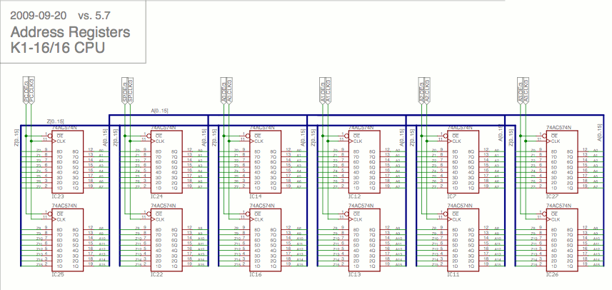
Address Registers Circuit

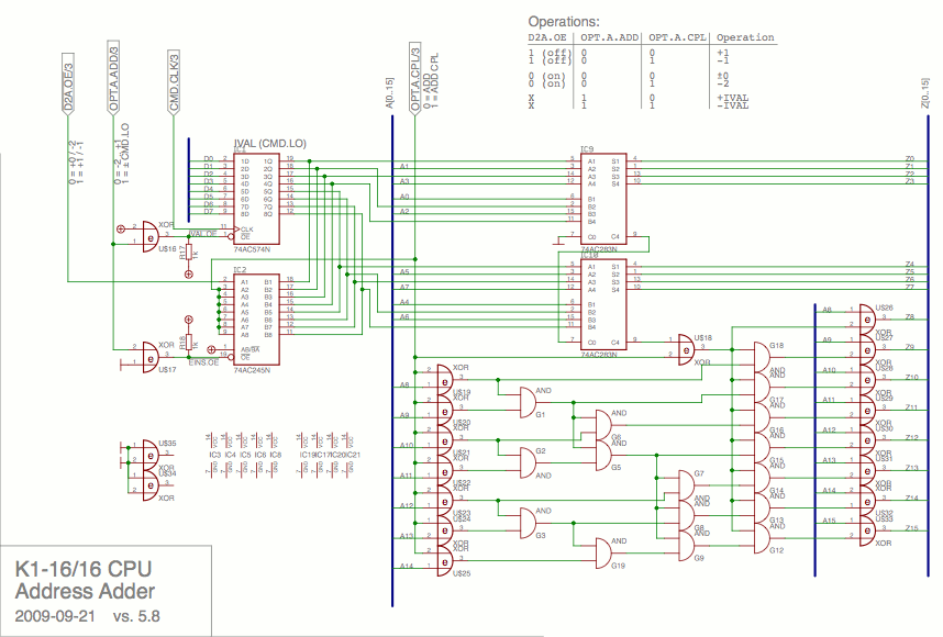
Address Adder Circuit
The address registers output their data to the address bus which is connected to the address lines of the built-in RAM of the CPU. Their inputs are connected to the address adder. They can only be loaded through the address adder, applying a non-zero address offset, except if they are loaded from the data bus across the data/address bus bridge, where the offset can be zero. The address adder can apply ±1 increment/decrement, +IVAL and +IVAL+$FF00, where IVAL is the low byte from the current instruction code. The up to 4 (6) possible operations are selectable by two option control lines from the control unit (and the state of the bus bridge output enable).
The address adder is a compromise between the wish to be able to add 8 bit displacements and the need for speed. If i had implemented 'my' pure ±1 increment adder, i would have saved ~ 2 gate delays (10ns in 74AC…) and this will probably have an impact on the maximum clock speed of about 20%.

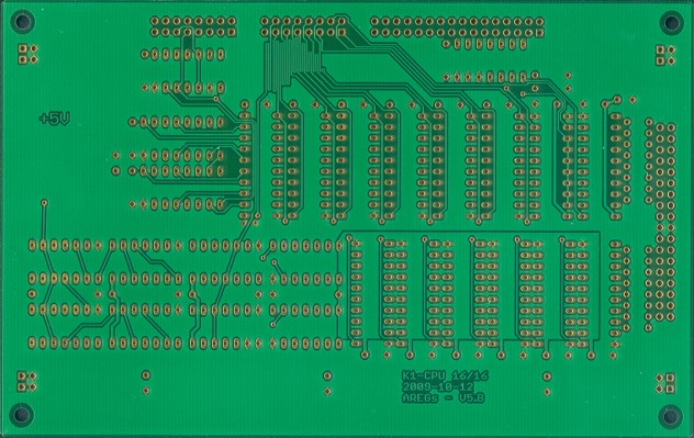
2009-11-03: Board arrived from LeitOn. Gold finish. :-) Bent. :-|
The serpentines are calculated to get roughly the same path lengths for the output enable control lines. On a FR4 board (which is what most PCBs are made from) the propagation speed of a signal is ~ 15cm/nsec, so a length deviation of 15 cm results in a signal delay of 1 ns. The 74AC… gates are switching within roughly 2 ns and have a propagation delay of typically 5 ns, so not too much effort is really needed here. After all this CPU will run at 16 MHz and not 3 GHz. :-) I just want to do my best for the output enable lines, because there is NO delay between switching them, just some meager efforts in pulse shaping for the control lines: the pull-up resistors on the control unit.
| Name | Letzte Änderung | Länge | |||
|---|---|---|---|---|---|
| Images/ | 2019-08-20 05:21 | 6 | |||
 |
AReg 5.8 - circuit adder.png size: 858 × 580 |
2009-09-21 21:49 | 43417 | ||
 |
AReg 5.8 - circuit registers.png size: 857 × 406 |
2009-09-21 14:12 | 34294 | ||
| AReg 5.B.brd | 2009-11-03 18:16 | 89611 | |||
| AReg 5.B.s#1 | 2010-01-22 15:15 | 111287 | |||
| AReg 5.B.s#2 | 2009-10-12 14:26 | 111287 | |||
| AReg 5.B.sch | 2010-01-28 20:43 | 111287 | |||
 |
component placement.png size: 786 × 492 |
2009-11-06 10:10 | 30813 | ||
| part list.txt | 2009-10-12 14:31 | 227 | |||
| signal length.txt | 2010-01-30 18:08 | 223 |
powered by vipsi - your friendly VIP Script Interpreter