
|
k1.spdns.de / Develop / Hardware / K1-Computer / K1-CPU / DRegs / |
 Overview
| Control Unit
| Microcode Header
| Arithmetic Unit
| Data Registers
| Address Registers
| Expansion Bus Overview
| Control Unit
| Microcode Header
| Arithmetic Unit
| Data Registers
| Address Registers
| Expansion Bus
|
|
|
k1.spdns.de / Develop / Hardware / K1-Computer / K1-CPU / DRegs / |
| Overview
| Control Unit
| Microcode Header
| Arithmetic Unit
| Data Registers
| Address Registers
| Expansion Bus
|
Work-in-progress – I'm currently reworking the project pages!
Some text on this page is in German only.
It will be translated to English some time later.
Last updated: 2012-05-03
Questions & comments to Kio
The last days i was working on the data registers board. The major problem was, to decide what actually will go on this board and how to wire up the RAM address and data lines. Now it's in a state where i think it is near finished. The ALU baord is still in production, and after that has arrived i will probably order the data registers and the address registers board in one go. The address registers board still had a bug. It's not bad to wait a week or two, so i can think over it all again.


The registers again are very straight forward. Input and output connect to their data line. This is basically the same for the shift and the byte swap registers too, except that the data lines for input and output are different here. The clock lines for some registers are strobed with the system's main clock CLK, because this is done for all registers on the control unit, except for 8 data registers, because i needed the unstrobed clock for I/O and RAM, and the colck lines are decoded in groups of 8 by the 74AC138 3:8 decoders. So i must strobe some of them (at most 6) explicitely on the data registers board.


The RAM circuit was a little bit tricky, because i enable the upper or lower RAMs based on an address line, and the switching must occur for both at the same time, or there will be data collission for some nano seconds. And, again, i added "strong" pull-ups to extend the inactive state slightly, so unavoidabe bus collission while switching (with no time gap) is reduced to a minimum. Let's see how it works.


Board after adding one gate delay to CY input of SL and SR
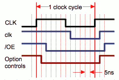 The CY input to the SR register mostly failed to read a '1'-bit. After scrutinizing the problem, i found out that the CY input goes away simulaneously with the clk signal for the register:
The blue clk is the load signal for the registers and the rising edge is where it latches new data from the data bus and, in case of data bit D15, from the CY line. The CY line is a 'option control' line, it controls options in the various registers, if they have. As can be seen in the image the option control line toggles exactly at the same moment (if it toggles) when the clk line raises.
So i had to delay the CY line. I inserted the unused OR gate from IC21 into the CY line and i hope the problem is now solved.
| Name | Letzte Änderung | Länge | |||
|---|---|---|---|---|---|
| Images/ | 2019-08-20 05:21 | 7 | |||
 |
component placement.png size: 786 × 492 |
2009-11-06 10:15 | 35427 | ||
| DReg 5.C.brd | 2009-11-03 18:16 | 100627 | |||
| DReg 5.C.s#1 | 2010-01-22 15:16 | 128335 | |||
| DReg 5.C.s#2 | 2009-10-12 13:07 | 128335 | |||
| DReg 5.C.sch | 2010-01-28 20:44 | 128335 | |||
|
DRegs 5.B circuit AxD, IVAL.png size: 878 × 620 |
2009-09-27 15:19 | 33152 | ||
|
DRegs 5.B circuit RAM.png size: 878 × 620 |
2009-09-27 15:18 | 29193 | ||
|
DRegs 5.B circuit registers.png size: 878 × 620 |
2009-09-27 15:18 | 22116 | ||
|
DRegs 5.B circuit shift, swap.png size: 878 × 620 |
2009-09-27 15:18 | 29045 | ||
| part list.txt | 2009-10-12 14:05 | 253 | |||
| signal length.txt | 2010-01-29 18:13 | 345 |
powered by vipsi - your friendly VIP Script Interpreter
![]()
![]()