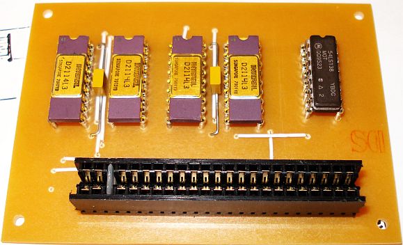
2K RAM pack for a total of 3K of RAM on the ZX80
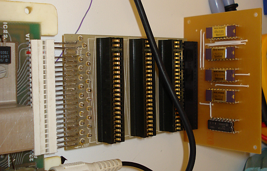
The finished RAM pack
One of the biggest problems with the ZX80 is it's small internal RAM. Most of the 1K RAM is consumed for the ZX80 operation and only a small portion is left for the user programs. The programs you can write with 1K are very basic and only a few 10s of BASIC lines are allowed to be written and run. There are few people that can write really sophisticated programs on the 1K and even fewer, like Paul Farrow, that can fit moving graphics games on the 1K. In order to do something more sophisticated, you have to have a hard time in programming or more RAM available. In this article I present you the complete construction of an external 2K RAM pack, which extends the internal RAM of the computer, for a total of 3K. This RAM pack was originally designed by V. Terrell for the ZX81 but works fine on the ZX80 too.
A RAM of 3K may not seem big at all considering today's standards and even the standards of 1980. In order to understand the usability of an additional 2K, think of the RAM size and what you can do with it, in terms of percentages. The additional 2K adds three times the available RAM of the computer. This means that you can write programs that are three times bigger in size. In fact, the benefit is even greater, as only a small portion of the internal 1K RAM is initially available for the user programs.
The "add on" RAM pack to be described gives the ZX80 an extra 2K of RAM. It works in conjunction with the ZX80 internal 1K of RAM, therefore providing a total of 3K of usable memory. All the necessary voltages and signals are readily available from the PCB dual finger-set at the rear of the ZX80, including it's power supply (5v). The unit simply plugs in and is immediately ready for use.
Memory store
The 2114 memory chips used in the unit can store 4-bit wide data at 1024 addresses. Because the ZX80 data bus is 8-bits wide, the four chips in the RAM pack are wired in pairs, each pair allowing data to be stored at 1024 addresses 8-bits wide.
Circuit operation
The complete circuit diagram for the RAM pack is shown below. The address lines A0-A9 are wired in parallel to the two pairs memory chips, IC1-4. These 10 lines carry information to call up any one of the 1024 address locations as selected by the computer. The eight lines D0-D7 carry data which can either be written (stored) into memory when the R/W (pin 10 on the IC) is low, this being controlled by the WR (write) line from the ZX80 (edge connector), or when this line is high, data may be read from the memory and processed by the computer.
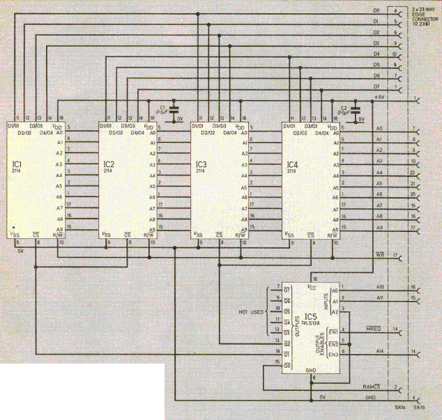
The two 1K memory blocks IC1, IC2, IC3 and IC4 are enabled only when their CS (pins 8 on the ICs) are low, a high will disable them. The ZX80 RAM starting address is 16384 and decoding is required to enable the RAM pack to be positioned 1K beyond this address.
Decoding
Address decoding for the extra RAM is accomplished using IC5, a three-to-eight line decoder IC with tristate outputs. The three inputs A0, A1 and A2 on IC5 form a three-bit binary number (eight decimal numbers). The output corresponding to the binary input goes to a logic low with the remainder at logic high. The decoding is not unique since and output will go low for the various combinations of 1s and 0s to the inputs, irrespective of the conditions of address lines A12 and A13, but does not need to be taken into account in this 2K system.
The IC, as stated earlier, is a tristate device which means that the outputs can be disenabled (effectively disconnected) by suitable control signals to the three enable pins EN1 (pin4), EN2 (pin5), EN3 (pin6) on IC5. The bar above EN1 and EN2, indicates that a low is required on them and a high on EN3 to "connect" the outputs to the following circuitry. A logic high on address line A14 means that the memory between 16K and 32K has been selected by the processor which is the requirement here. When addressing memory for read or write, the processor generates a low on MREQ (edge connector) at a time when the address bus is stable. Thus addressing memory above 16K causes one of the outputs Q0 to Q2 to reach the RAM ICs. This is summarized in the picture below. Q3 is not used.
| Inputs | Outputs | Chip enabled | |||||
| A14 | MREQ | A10 | A11 | Q0 | Q1 | Q2 | |
| 1 | 0 | 0 | 0 | 0 | 1 | 1 | XZ80 Internal RAM |
| 1 | 0 | 1 | 0 | 1 | 0 | 1 | IC1, IC2 (First extra 1K) |
| 1 | 0 | 0 | 1 | 1 | 1 | 0 | IC3, IC4 (Second extra 1K) |
If A14 is low or MREQ high, all outputs are high impedance
Truth table
The truth table for the decoder (IC5) reads as follows: When Q0 is high the internal 1K RAMCS pin is disenabled. Q1 low enables the CS pins (pins 8) of IC1 and IC2, selecting the first 1K of memory. Q2 low enables the CS pins (pins 8) of IC3 and IC4 selecting the second 1K of memory. Decoupling capacitors C1 and C2 are required for each RAM pair to filter away any transients that may occur on the supply rail.
Construction
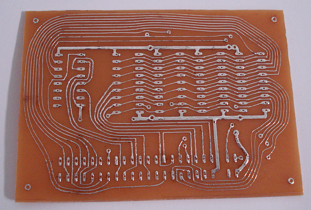
The RAM pack PCB layout files are shown below. The PCB layout in the old magazine article was not good. The scan was of very low quality and apart from that, many lines where too close together to be able to correctly print on a PCB. All these problems were corrected by reverse engineering and image editing techniques.
RAM pack PCB layout in PDF format 600 dpi (prints in correct scale)
Components list:
| Component No | Type | Qty | Mil./Indust. or better equivalent |
| IC1-IC4 | 2114 SRAM | 4 | D2114L-2 or D2114L3 Ceramic side brazed version |
| IC5 | 74LS138 | 1 | 54LS138 |
| SK1 | Modified ISA bus connector | 1 | |
| Wire bridges | 10 | Tensolite Carlisle Co. Silver Coated Copper Wire 30 AWG Solid, White PTFE Jacket, 600V @ 200°C, P/N: 63111BD30BNN5 | |
| C1, C2 | 0.1uF | 2 | M39014/01-1553 |
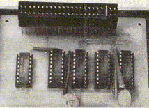
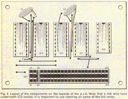
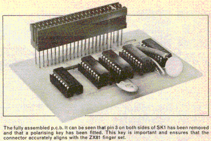
The placement of the components can be seen on the next pictures
After etching, the PCB has to be soldered and drilled.
The original RAM pack uses a connector with long pins. These connectors are obsolete, so I have decided to use an ISA bus connector with short pins, that has been cut accordingly to fit the ZX80 bus. This connector fits right onto the PCB in contrast with the original connector that stands a few cm above the PCB. This makes the RAM pack difficult to fit into a boxed ZX80, but it makes no difference if fit into a bare ZX80 PCB.
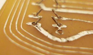
When the time comes to solder the connector, pass the connector pins through the holes and bend them slightly inwards as shown in the next photo. The reason for bending the connector pins is to support the expansion bus later on, if you decide to make another expansion card.
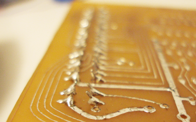
Then solder the connector pins to the PCB as shown in the next photo.
The Last thing you have to do about the connector is to insert the key to it. I used a piece of plastic material to make the key and I slipped it in the "empty pin" place of the connector, as shown on the left hand side of the picture below. You can also use a piece of thin PCB or anything else you like as a key.

The wire bridges have to be soldered next. The picture in the beginning of this page clearly shows where the wire bridges should be soldered. The little wire bridge near the connector, cannot slip under it, so this has been soldered at the back of the PCB. This wire bridge is shown at the top left of the next picture.

The back side of the PCB
Testing
To test the RAM pack, I used the Maplin bus to extend the bus of an original ZX80. Then I plugged in the RAM pack at the end of the expansion bus.
According to the magazine the unit can be easily tested by using the ZX80 "ramtop" test. Plug the unit in, then switch the ZX80 on and type in the following:
PRINT PEEK 16388 + 256 * PEEK 16389 NEW LINE
You should see 19456 displayed on the screen. The result 19456=16384+3K of RAM. This short program retrieves and displays the contents of locations 16388 and 16389 which contain the least and most significant bits respectively of the address plus 1 of the highest RAM location in circuit. This information has been "poked" into these locations during the system set-up routine which is initialized at switch-on.
In my case, this routine did not work as expected (maybe this is due to the use of the 4K ROM), so I decided to try loading 3K programs into the RAM, to see if they could load. First I tried to load 3K programs without fitting the RAM pack. The computer crashed as it was expected. Then I fitted in the RAM pack and tried to load these 3K programs again. They were loaded ok.
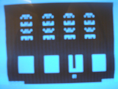
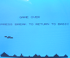
The pictures above show the 3K space invaders game and the defenda game, successfully loaded into the ZX80 fitted with the RAM pack.
Martin sent me another routine for testing the RAM pack too.

Press RUN and then New Line, to run the routine. The result should be 3072, which is the total RAM of the computer.